Abstract
A minimalist shortwave regenerative receiver circuit is presented that is powered by a 1.2-volt cell and uses exclusively 2N3904 transistors. Tuning is accomplished by a 1SV149 hyperabrupt varactor powered by a separate 9-volt supply. The receiver design emphasizes simplicity and exhibits good operational performance including smooth regeneration control, frequency stability, and sensitivity sufficient to hear HF band noise. Key aspects of the receiver's behavior are analyzed using LTspice. Several references are provided, both to explain aspects of the presented design, and to show more advanced designs.
Introduction
The goals of this project were as follows:
- Design and implement a minimalist but practically usable regenerative receiver capable of HF reception from 3-30 MHz.
- Analyze the key aspects of the receiver's operation (e.g. behavior of the regenerative detector, gain and frequency response of the AF amplifier) using the circuit simulation tool LTspice.
- Write this article explaining the design and explaining the LTspice analysis techniques in enough detail such that the interested reader can reproduce the simulation results. Also, provide several references to improved designs for regenerative detectors or regenerative receivers.
Minimalist constraints
The following constraints were chosen to keep the design a minimalist design.
- Only 2N3904 transistors should be used.
- The power for the transistors should come from a 1.2-volt cell.
- The receiver should be built as physically small as possible, preferably small enough to fit in a pocket.
Why 2N3904 transistors?
2N3904 transistors are commonly and cheaply available, aiding reproducibility of the design. Their transition frequency is high enough to allow them to serve as oscillators over the entire HF spectrum. At the same time, their transition frequency is low enough so that they don't tend to oscillate spuriously at VHF or UHF. And, I have several on hand.
Why 1.2 volts?
A 1.2-volt AAA cell is the smallest generally-available, general-purpose, rechargeable cell, and I prefer using rechargeable rather than disposable batteries to power my receivers. Given the minimalist goals of the receiver and the additional goal of small physical size, a 1.2-volt AAA cell was the natural choice for the power supply. Restricting the receiver to be powered off of a single cell rather than a pack of several cells again helps keep the physical size of the receiver small, as well as greatly simplifies the process of removing, charging, and replacing the battery; it would be tedious to individually charge and replace several cells at once. Also, using a single cell for power might allow for the possibility of in-situ battery charging, via for example a solar cell. Finally, it is an interesting exercise to design a receiver with sufficient intput-to-output gain (approximately 100 dB) that is powered by a single low-voltage cell.
Why a physically small receiver?
The reason for constraining the design to be physically small is to allow the set to be easily taken on trips or in the field. A small physical size encourages more frequent use of the receiver in various situations. Also, designing a physically small HF receiver is an interesting challenge to ensure good RF behavior (no unwanted output-to-input couplings or unwanted oscillations) and a convenient physical circuit layout allowing practical operation of the physical controls.
Practical use constraints
To enable the receiver to be usable in practice for listening to a variety of signals on various HF bands, the following constraints were defined.
- To allow both a wide tuning range and a comfortably slow tuning rate, in a physically small package, tuning should be done with a 1SV149 hyperabrupt varactor connected to a ten-turn potentiometer.
- To prevent detuning effects from hand capacitance or variations in antenna impedance, an isolating RF stage should be included.
- To make best use of the receiver's dynamic range, a passive RF attenuator should be included.
- The operation of the regeneration control must be smooth, free from hysteresis, and free from squegging, motorboating, super-regeneration, or fringe howl.
- To allow easy band-switching, the coil should be a 2-terminal coil with no taps or secondary windings.
- The receiver must be able to operate from 3-30 MHz without changing any components except for the tank inductor.
Non-constraints
No receiver design is perfect. The below list enumerates some "imperfect" aspects of this article's receiver design that were considered for improvement, but that were ultimately excluded from the scope of this design.
Use of a single-active-device regenerative detector
No attempt is made to separate Q-multiplication, detection, and amplitude limiting into separate stages, instead relying on the “classical” single-active-device topology that requires that single active device to be responsible for linear signal amplification, non-linear detection, and self-limiting amplitude behavior as the regeneration control is increased past the oscillation threshold. Distributing the above functions onto separate active devices in general allows a higher-performance receiver, as each active device can be optimally biased and parameterized for its particular function (linear signal amplification, non-linear detection, or non-linear gain compression). Achieving such a high level of performance was not a goal of this project.
However, for examples of higher-performance designs, see for example Ref. 1 (references are provided at the end of this article), which separates the Q-multiplier and detector stages (using a hybrid cascode detector stage). For an even more involved design, see Ref. 2 and Ref. 3, which describes a design that separates the Q-multiplier, detector, and gain compressor into three separate stages, and furthermore implements some unique optimizations in the gain compressor, using a scale-invariant gain compression law, to allow a never-before-seen capability to control (above the oscillation threshold) both the Q-multiplier bandwidth and the oscillation amplitude independently of one another; normally, in a single-active-device regenerative detector, bandwidth and oscillation amplitude cannot be independently adjusted and are tied together due to the implicit, poorly-characterizable, and scale-varying self-limiting behavior of the active device as it enters class C operation when pushed far above the oscillation threshold.
Tank loading by the transistor
Only minimal attention is given to minimize tank loading by the transistor. The chosen oscillator topology, described later in this article, depends on transistor saturation for its amplitude-limiting behavior, which will (a) reduce tank Q and (b) introduce noise.
Regarding point (b) of noise introduction due to saturation, this essentially does not matter in a regenerative detector intended for HF use because the HF band noise will be stronger than the detector noise (Ref. 4).
Regarding point (a) of reduction of tank Q due to saturation, this effect may matter in that it broadens the tank's Q-multiplied bandwidth at critical threshold. However, the tank Q is already being reduced due to another factor -- the design choice to use a 1SV149 varactor for the tank capacitance. This varactor, intended for MW use, introduces at HF frequencies noticeable loss into the tank (noticeable in that the regeneration level required to reach threshold is higher than when a variable capacitor is used), which is to be expected as this varactor's Q will be only about 20 at 10 MHz (Ref. 5, Ref.6). Since the tank's Q is already relatively low due to the low varactor Q, the possible improvement in tank Q achievable by reducing transistor loading is probably small in comparison to the varactor losses, though no measurements were made to confirm this assumption. Furthermore, reducing transistor loading would require a more complex biasing scheme, a more complex (tapped) inductor, a higher supply voltage, and/or a separate detector stage (due to poor detection efficiency of the rebiased q-multiplier) -- all of which go against the minimalist nature of this project.
Fidelity of AF amplifier
No attempt was made to design a high-fidelity and low-distortion AF amplifier. Instead, the AF amplifier (which, like the rest of the receiver, runs off of 1.2 volts) was designed simply to have enough gain from low to moderate AF frequencies, with no concern for fidelity.
Background and Related work
V. Polyakov, in his book on homebrew receivers (Ref. 7), presented a very simple regenerative receiver design based on a Hartley oscillator, whose design served as an inspiration for the design of this article's regenerative detector circuit.

The circuit's operation is described in the References 8, 9, and 10. Below we review some of the particular features of this regenerative detector.
Biasing of Polyakov's regenerative detector and AC amplification
Perhaps the most notable aspect of this circuit is its biasing, which allows an extremely low parts count and operation at low voltages. The biasing sets both the collector and the base at the same DC voltage. However, even in this state, the transistor can still amplify AC signals (Ref. 9, Ref. 11).
The following circuit simulation, carried out in the LTspice circuit simulator, verifies the AC amplification of this circuit (note the below circuit uses an NPN transistor in contrast to Polyakov's original PNP transistor). In the below circuit, the regenerative detector has been modeled, but the feedback loop has been broken open at the base. Normally, the base would be connected to the node labeled "feedback," which allows the base to receive its bias voltage through the small feedback coil L2. Instead, in this open-loop simulation, the base is tied directly to Vcc, and a new AC voltage source V2 is inserted at the base to simulate the effect of incoming signals perturbing the base bias. R2 has been added to represent coil loss.

First, we run a frequency domain analysis, also called an AC analysis, to measure the AC response of the amplifier. As explained above, the amplifier input for the simulation is at the base. We measure the amplifier output at the open end where we broke the feedback loop, i.e., at the node named "feedback," after the amplifier has amplified the input signal and sent it through the resonator. The frequency is swept from 1 MHz to 15 MHz. The amplifier's frequency response curve is plotted for various values of the regeneration control (emitter resistance) from 100 ohms to 50k ohms.
The result of the AC analysis is shown below.

At low emitter resistance we see significant gain of around 30 dB (the green curve). As emitter resistance increases, AC gain of the amplifier decreases. As long as the amplifier's output at the node "feedback" is sufficient to overcome the coil losses, we will have enough gain for oscillation.
For example, the blue curve in the above graph illustrates that with an emitter resistance of 10.1k, peak gain of approximately 13 dB occurs at 4.758 MHz. To double-check the AC amplification properties of the transistor, the following transient (time-domain) analysis was run, exciting the tank with a 1 microvolt signal at the tank's resonant frequency of 4.758 MHz.

The results of the transient analysis appear below. The green trace is the input signal at the base -- a steady 1 microvolt over the entire time of the simulation. The blue trace is the output signal measured at the "feedback" node. As expected, it slowly grows in amplitude over time as the continued rhythmic variations of the input signal pulse in phase with the natural oscillation of charge in the tank at 4.758 MHz. The natural amplification of the tank is assisted by the amplification of the transistor. The final steady-state amplitude of the amplified signal is about 4.5 microvolts, which is 4.5 times the input amplitude of 1 microvolt. And a voltage amplification of 4.5 times equals approximately a 13 dB amplification (voltage gain in dB = 20 × log (V2 / V1)), which is the same result we obtained from the AC analysis.


It is also possible to conduct more detailed analyses in LTspice such as estimating the actual value of the regeneration control (emitter resistance) required to reach the oscillation threshold, estimating the smoothness of regeneration control, or evaluating the detection efficiency of the regenerative stage. Future articles can explore these topics if there is interest.
Note that the above simulations omitted any magnetic coupling between the two coils L1 and L2. In Polyakov's original design the two coils L1 and L2 are formed by a single tapped coil, implying magnetic coupling between L1 and L2. However, since this is a Hartley oscillator, no magnetic coupling between L1 and L2 is needed. This seems surprising or even unbelievable to some experimenters, for which reason I prepared the following video demonstrating the above oscillator circuit oscillating with two separate, non-magnetically-coupled coils. In any event, the presence or absence of magnetic coupling does not affect the validity of the above simulations that illustrate the AC amplification capability of the Polyakov regenerative detector.
Video illustrating non-necessity of magnetic coupling in Polyakov-style Hartley oscillator.
Biasing of Polyakov's regenerative detector and Vce stability
An additional property of the biasing of Polyakov's circuit is voltage stabilization (Ref. 12). The voltage across the transistor is relatively stable even as the regeneration control (emitter resistance) is adjusted. This voltage stability means that the transistor's parasitic capacitances are also mostly stabilized, meaning that there is little frequency shift when adjusting the regeneration control around threshold.
The following circuit simulation illustrates the stability of the collector-emitter voltage Vce as the regeneration control is adjusted. Below is a model of the Polyakov regenerative detector at DC. At DC, the base and collector are tied to Vcc, since the DC impedance of the tank inductor is 0 at DC. Furthermore, at DC, all of the capacitors are open circuits and can be ignored.

The above simulation parameters are configured to vary the emitter resistance from 1 ohm to 10k ohms. (In the physical circuit described later in this article, it was verified that 10k was a plausible value to reach the oscillation threshold.) Also, the battery voltage is varied from 1.3 volts to 1.0 volts, to represent lower supply voltage as the battery is depleted over time.
For the above simulation parameters, the collector-to-emitter voltage is graphed below.

Note that even as the regeneration control and the supply voltage vary over reasonable ranges, the collector-to-emitter voltage stays relatively constant around 600 mV. And the base and collector are tied to the supply voltage, remaining constant. So all the transistor voltages are stabilized, leading to the reduced frequency shift when the regeneration control is adjusted around threshold.
One superficially detrimental aspect of Polyakov's detector circuit is that the oscillator depends on driving the transistor into saturation for part of the oscillation cycle. The transistor enters saturation if the base-collector diode becomes forward biased, which then presents a low impedance to the collector (Ref. 13, Ref. 14) and damps the tank, introducing noise and harmonic energy in the process. Reference 15 describes the saturation mechanism of a very similar oscillator.
The saturation process can also be intuitively understood by considering that as oscillation commences, the opposite ends of the tank inductor alternately go positive and negative, and since the opposite ends of the tank are both biased to be at the same Vcc voltage, the oscillating voltage necessarily causes, for half of the oscillation cycle, a forward biasing of the base-collector junction, which is equivalent to placing a forward-biased, low-impedance diode across the high-impedance tank.
The below transient simulation verifies the saturating behavior of the Polyakov detector in the oscillating condition. Current source I1 has been added to the simulation to "kick start" the oscillator by providing a momentary current pulse at the start of the simulation. This allows the oscillator to reach its final steady-state amplitude faster.

The transient simulation results are as follows. The red trace is the collector-to-base voltage, which for half of the cycle dips below 0 volts, indicating the base voltage is higher than the collector -- a saturation condition that lowers the collector impedance and introduces noise into the tank.

In an isolated oscillator this noise might be worth worrying about. But, as stated above in the "Non-constraints" section and in Reference 4, in a regenerative detector, this oscillator noise is insignificant compared to the band noise (from the antenna) that we are injecting into the oscillator anyway. So as long as we can hear the band noise, it's not worth worrying about the oscillator noise introduced by transistor saturation.
Biasing of Polyakov's regenerative detector and saturation/noise
One superficially detrimental aspect of Polyakov's detector circuit is that the oscillator depends on driving the transistor into saturation for part of the oscillation cycle. The transistor enters saturation if the base-collector diode becomes forward biased, which then presents a low impedance to the collector (Ref. 13, Ref. 14) and damps the tank, introducing noise and harmonic energy in the process. Reference 15 describes the saturation mechanism of a very similar oscillator.
The saturation process can also be intuitively understood by considering that as oscillation commences, the opposite ends of the tank inductor alternately go positive and negative, and since the opposite ends of the tank are both biased to be at the same Vcc voltage, the oscillating voltage necessarily causes, for half of the oscillation cycle, a forward biasing of the base-collector junction, which is equivalent to placing a forward-biased, low-impedance diode across the high-impedance tank.
The below transient simulation verifies the saturating behavior of the Polyakov detector in the oscillating condition. Current source I1 has been added to the simulation to "kick start" the oscillator by providing a momentary current pulse at the start of the simulation. This allows the oscillator to reach its final steady-state amplitude faster.

The transient simulation results are as follows. The red trace is the collector-to-base voltage, which for half of the cycle dips below 0 volts, indicating the base voltage is higher than the collector -- a saturation condition that lowers the collector impedance and introduces noise into the tank.

In an isolated oscillator this noise might be worth worrying about. But, as stated above in the "Non-constraints" section and in Reference 4, in a regenerative detector, this oscillator noise is insignificant compared to the band noise (from the antenna) that we are injecting into the oscillator anyway. So as long as we can hear the band noise, it's not worth worrying about the oscillator noise introduced by transistor saturation.
A modified Polyakov-style circuit based on a Vackar-style oscillator
For the development of the minimalist regenerative receiver in this article, the above Polyakov design was considered as a starting point. The basic concepts were kept of holding the base and collector at the same DC voltage, and of using emitter resistance to control regeneration. However, in the current design, the tapped coil (or separate coils) required by the Hartley oscillator was replaced by a single, non-tapped coil, and the feedback arrangement was altered to become a Vackar-style oscillator using a pi feedback network to achieve the necessary output-to-input phase shift.
The circuit diagram is presented below, and the following subsections describe the parts of the circuit in detail.

The circuit diagram is presented below, and the following subsections describe the parts of the circuit in detail.

The Vackar-style regenerative detector Q2
The regenerative detector (Q2 in the above circuit diagram) is based on a Vackar oscillator, but differs from a true Vackar oscillator in two ways.
First, the high-impedance end of the tank inductor is fully coupled into the active device (at the collector) instead of using a fractional-coupling, capacitive-divider arrangement as in the true Vackar oscillator.
Second, the capacitor C12 at the low-impedance end of the tank inductor is of higher impedance than is recommended in true Vackar oscillators. C12 has a compromise value chosen experimentally to allow enough feedback over the entire 3-30 MHz range. Ideally, it should be 10x larger than the largest value of the variable capacitance D1, which is ~500 pF for the 1SV149 varactor, meaning C12 should be about 5000 pF to make the top of C12 (base side of L1) much lower impedance than the "hot" end of the tank (top of D1/collector side of L1). The problem with making C12 too large though is that its impedance becomes so small that likely there will not be enough feedback for oscillation (or smooth transition into oscillation) on the high band 9-30 MHz (when L1 is small). On the other hand, the problem with making C12 too small is that it raises the impedance at the base-side of L1, thus introducing an impedance mismatch between the somewhat-high impedance point at the top of C12 and the low-impedance transistor base, leading to tank damping and parasitic capacitance as the base is more tightly coupled into the tank. Another problem with making C12 too small is that the raised impedance more tightly couples the RF amp Q1 into the tank, whereas ideally this coupling should be quite light. So, it's clear that by using only a single C12 value (to cover 3-30 MHz with different values for L1), its value must be a compromise.
Dual function of radio-frequency choke L2: Floating at RF, but grounded at AF
The radio-frequency choke L2, with a value of 3.3mH, is being used above its self-resonant frequency. The datasheet at Ref. 16 shows that the typical self-resonant frequency of a 3.3 mH choke is around 700 kHz, whereas Q2's oscillation frequency will be significantly above this, somewhere from 3 MHz to 30 MHz. This means that the choke's apparent reactance in the circuit is actually capacitive instead of inductive. Fortunately, in this circuit, this doesn't matter because the capacitive reactance of L2 just appears to be an additional small (but frequency-dependent) capacitance in parallel with C12.
To enable the required RF feedback signal to be fed into the base, L2's moderately high (though capacitive) reactance at RF serves to hold the base-end of tank inductor L1 above ground at RF. At the same time, L2's low reactance at AF also serves to hold the base-end of the inductor at ground at AF. This helps prevent 50 Hz hum pickup (from surrounding household wiring) by the tank inductor by shunting such low-frequency signals to ground. For example, a 3.3 mH choke will have a reactance of only about 1 ohm for 50 Hz signals, effectively preventing hum pickup by the base-end of the tank inductor. If, on the other hand, the base-end of the tank inductor L1 were floating at AF, this could make the detector susceptible to hum pickup. Such a situation (floating L1) would occur if Q2's base were biased through high-value resistors instead of an RFC. See Ref. 17 for an example of such a hum-susceptible Vackar-style regenerative detector.
Tuning range and bandswitching
L1 is currently about 25 turns on a T50-6 (yelllow) toroidal core. With this inductor, the set oscillates from about 4-16 MHz, with a smooth transition into regeneration. By replacing L1 with an inductor having only 12 turns on a T50-6 core, it was verified that the circuit oscillated up to 30 MHz and still still behaved well with a smooth transition into regeneration and a clean oscillator signal, as monitored on a nearby receiver.
Though oscillator behavior was tested on the high band of 9-30 MHz, actual reception tests have not yet been performed on the high band with the smaller inductor. The current low-band coil is permanently soldered into the circuit, making bandswitching tedious. In the future this receiver will be modified to allow easier bandswitching of the coil L1, at which point actual reception tests will be done on the high band of 9-30 MHz.
Although it is possible to switch both ends of L1 among different coils for bandswitching, it is also possible to use a single coil with multiple taps, and to to switch only one end of L1 (preferably, the low-impedance base-end) among the multiple taps. When a tap is switched into the circuit, the extra unused turns of the inductor are simply left floating and unused. Experiments with a tapped T50-6 coil confirmed that extra floating turns (when a coil tap rather than the full coil is switched into the circuit) did not have any effect on the operation of the regenerative detector. Such a tapped-coil arrangement allows a single coil to cover multiple bands, which might make for a more compact bandswitching implementation than a scheme using multiple coils.
Though oscillator behavior was tested on the high band of 9-30 MHz, actual reception tests have not yet been performed on the high band with the smaller inductor. The current low-band coil is permanently soldered into the circuit, making bandswitching tedious. In the future this receiver will be modified to allow easier bandswitching of the coil L1, at which point actual reception tests will be done on the high band of 9-30 MHz.
Although it is possible to switch both ends of L1 among different coils for bandswitching, it is also possible to use a single coil with multiple taps, and to to switch only one end of L1 (preferably, the low-impedance base-end) among the multiple taps. When a tap is switched into the circuit, the extra unused turns of the inductor are simply left floating and unused. Experiments with a tapped T50-6 coil confirmed that extra floating turns (when a coil tap rather than the full coil is switched into the circuit) did not have any effect on the operation of the regenerative detector. Such a tapped-coil arrangement allows a single coil to cover multiple bands, which might make for a more compact bandswitching implementation than a scheme using multiple coils.
RF amplifier Q1
Q1 serves as a common-base RF amplifier. The collector load is provided by RFC L2, which conveniently also supplies Q1's collector voltage. The base is effectively tied to Vcc, thus allowing the emitter resistance to set the current through Q1. Emitter current always flows through the full resistance of VR1, which is 100 ohms.
Note that the voltages at the Q1 collector and base are not the full Vcc voltage of 1.2 volts, but are instead intentionally reduced by the voltage drop across R11 (described in the following subsection about the AF amp). Accounting for the voltage drop across R11, the voltages at the Q1 collector and base are approximately 936 mV according to an LTspice analysis.
With 936 mV at the base/collector and an emitter resistance of 100 ohms, an LTspice analysis indicates 2.56 mA of current continuously flowing through Q1. This closely aligns with the value of 2.5 mA recommended in Ref. 18 for a common-base amplifier. However, it should be noted that the circuit in Ref. 18 used a supply voltage of 6 volts or above, whereas the circuit of this article uses only 1.2 volts, meaning that Ref. 18's recommendation of 2.5 mA might further be optimized for the circuit of this article. In particular, Ref. 18 implies that the important value may be not the current through Q1 but rather the voltage across Q1's emitter resistor, which should be large relative to the expected maximum signal strength at the antenna in order to avoid overload. This in turn implies that the Q1's current should be set as high as needed to achieve the required voltage across Q1's emitter resistor.
The wiper on VR1 serves as an RF attenuator and allows a portion of the incoming antenna signal to be shunted to ground.
Q3 is an emitter-follower stage that has high AF input impedance and serves to isolate the detector Q2 from the following common-emitter stages Q4-Q7. If Q3 is omitted, and for example C10 is connected directly to C11, then C2 will effectively be in parallel with C11, leading to a quite large capacitance across VR4. This high capacitance can lead to super-regeneration, because the high capacitance allows a high voltage to build up across VR4, with VR4 being unable to discharge the capacitance completely before the next oscillation cycle. This gradual buildup of charge across VR4 eventually raises the emitter voltage so high that the transistor gain is reduced and oscillation is, momentarily, halted. After oscillation halts, VR4 discharges the capacitance, and again oscillation commences, until the charge buildup again halts it.
In practice this periodically-interrupted oscillation manifests itself as an AF oscillation when the regeneration control is adjusted near critical threshold. Interestingly, it is possible to exploit this property to achieve an automatic regeneration control by rectifying the AF oscillation and using it as a control voltage to back off the regeneration (Ref. 19). (An alternative means of achieving automatic regeneration control, operating on the RF signal directly, is described in Ref. 20.)
Preventing the above super-regenerative behavior can also be done by inserting a resistance between C10 and C11 (e.g., Ref. 21). However, sufficient isolation requires a high value of isolating resistance, and this in turn has the undesired side effect of reducing the AF signal voltage available for subsequent amplification. Using the emitter follower Q3 causes no loss of AF signal voltage while still achieving good isolation between the detector Q2 and the following AF stages.
The biasing of Q3, achieved through resistor R10, has not been carefully designed. The quiescent voltage at the Q3 base is probably not optimal, which might limit the dynamic range of Q3. However, the input AF signal levels fed into the Q3 base will be very low anyway, so overload of Q3 is probably unlikely.

In practice, sufficient AF gain was confirmed by connecting the regenerative detector's AF output to the input of the AF amplifier. Using a piezoelectric crystal earphone connected to the amplifier output, the regenerative detector's threshold noise could be clearly heard as the regeneration control was advanced towards threshold. Being able to clearly hear the regenerative detector's threshold noise indicates in practice that the AF amp has enough gain.
The AF amplifier also can drive low-impedance (32-ohm) consumer-grade headphones. In this case, the resulting audio level is quite low, but listenable. It is also possible to connect the AF output to the microphone-in or line-in of an external amplifier, for increased output power or making a recording of the receiver's audio (as was done for the video shown later in this article).
An initial prototype of the AF amplifier, constructed according to the above circuit diagram, showed some tendency for self-oscillation. This could be verified by tying the input of the amplifier to Vcc, which immediately caused an audible AF oscillation at the amplifier output.
The root cause of this instability is the later stages of the AF amplifier being able to ripple the Vcc voltage by a small amount, and in-phase with the input signal. This in-phase ripple travels over the Vcc line back to the input of the amplifier, causing positive feedback and AF oscillation. To remedy this situation requires decoupling the earlier AF stages from the later AF stages to prevent such Vcc ripple from traveling back across the Vcc line. Such decoupling can be achieved with a series resistor and capacitor at the first AF amplifier transistor, essentially forming a separate Vcc supply for the first AF amplifier and the rest of the receiver (Ref. 22).
For the receiver circuit of this article, the AF amp decoupling is achieved by R11 and C14.
Good RF design practice would place an additional RF bypass capacitor across C14 to ensure a sufficiently low-impedance path for RF signals and prevent RF from traveling into the Vcc supply line where it might cause instability. High-value electrolytic capacitors like C14 may not have sufficiently low impedance at RF. Nevertheless, in this circuit, such additional RF bypassing was omitted for simplicity, and C14 by itself seems to function adequately as an RF bypass.
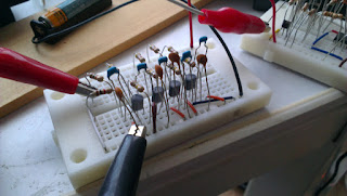
Construction began with the low-voltage AF amp. First, the AF amp was prototyped on a solderless breadboard.
Then, a compact version of the AF amp was built. The collector feedback bias resistor and RF bypass capacitor were soldered directly to each transistor.

The four transistors were then soldered together to form the four-stage amplifier. An LM386 chip is shown as a size comparison.

The AF amp could be soldered into and out of the circuit as an integrated unit. In the below photograph, the prototype receiver's detector stage is constructed on a copper ground plane, while the AF amp is soldered as an integrated unit onto the detector.

After the detector design (including a preceding RF amp and a following AF buffer) was finalized, the additional transistors were soldered directly to the AF amp to make for a maximally-compact build. In the photograph below, the left three transistors are the RF amp, regenerative detector, and AF buffer, respectively. The right-most transistors are the AF amplifier.

With the basic receiver components in place, the tank inductor L1 and the controlling potentiometers were soldered into the circuit, and the whole circuit was placed inside a small plastic box. Ten-turn potentiometers, with turns-counting dials, were used for the tuning potentiometers VR2 and VR3. The turns-counting dials allow a reasonable degree of repeatability in tuning. A ten-turn potentiometer is also used to control the regeneration, allowing a high resolution of adjustment.

The final receiver looks as shown in the following two photographs.

Note that the voltages at the Q1 collector and base are not the full Vcc voltage of 1.2 volts, but are instead intentionally reduced by the voltage drop across R11 (described in the following subsection about the AF amp). Accounting for the voltage drop across R11, the voltages at the Q1 collector and base are approximately 936 mV according to an LTspice analysis.
With 936 mV at the base/collector and an emitter resistance of 100 ohms, an LTspice analysis indicates 2.56 mA of current continuously flowing through Q1. This closely aligns with the value of 2.5 mA recommended in Ref. 18 for a common-base amplifier. However, it should be noted that the circuit in Ref. 18 used a supply voltage of 6 volts or above, whereas the circuit of this article uses only 1.2 volts, meaning that Ref. 18's recommendation of 2.5 mA might further be optimized for the circuit of this article. In particular, Ref. 18 implies that the important value may be not the current through Q1 but rather the voltage across Q1's emitter resistor, which should be large relative to the expected maximum signal strength at the antenna in order to avoid overload. This in turn implies that the Q1's current should be set as high as needed to achieve the required voltage across Q1's emitter resistor.
The wiper on VR1 serves as an RF attenuator and allows a portion of the incoming antenna signal to be shunted to ground.
AF buffer stage Q3
Q3 is an emitter-follower stage that has high AF input impedance and serves to isolate the detector Q2 from the following common-emitter stages Q4-Q7. If Q3 is omitted, and for example C10 is connected directly to C11, then C2 will effectively be in parallel with C11, leading to a quite large capacitance across VR4. This high capacitance can lead to super-regeneration, because the high capacitance allows a high voltage to build up across VR4, with VR4 being unable to discharge the capacitance completely before the next oscillation cycle. This gradual buildup of charge across VR4 eventually raises the emitter voltage so high that the transistor gain is reduced and oscillation is, momentarily, halted. After oscillation halts, VR4 discharges the capacitance, and again oscillation commences, until the charge buildup again halts it.
In practice this periodically-interrupted oscillation manifests itself as an AF oscillation when the regeneration control is adjusted near critical threshold. Interestingly, it is possible to exploit this property to achieve an automatic regeneration control by rectifying the AF oscillation and using it as a control voltage to back off the regeneration (Ref. 19). (An alternative means of achieving automatic regeneration control, operating on the RF signal directly, is described in Ref. 20.)
Preventing the above super-regenerative behavior can also be done by inserting a resistance between C10 and C11 (e.g., Ref. 21). However, sufficient isolation requires a high value of isolating resistance, and this in turn has the undesired side effect of reducing the AF signal voltage available for subsequent amplification. Using the emitter follower Q3 causes no loss of AF signal voltage while still achieving good isolation between the detector Q2 and the following AF stages.
The biasing of Q3, achieved through resistor R10, has not been carefully designed. The quiescent voltage at the Q3 base is probably not optimal, which might limit the dynamic range of Q3. However, the input AF signal levels fed into the Q3 base will be very low anyway, so overload of Q3 is probably unlikely.
AF amplifier Q4-Q7
Q4-Q7 simply form a series of common-emitter stages with collector feedback bias.
Gain of AF amplifier
The 4 stages should provide approximately 90 dB of gain at audio frequencies from around 200 Hz to 10 kHz, as shown in the below LTspice simulation. Gain drops off sharply after 10 kHz thanks to the 10 nF capacitors tying each transistor's base to ground at RF. Reduced gain at RF helps ensure amplifier stability by preventing amplification of stray RF signals that might make their way into the AF amplifier.

In practice, sufficient AF gain was confirmed by connecting the regenerative detector's AF output to the input of the AF amplifier. Using a piezoelectric crystal earphone connected to the amplifier output, the regenerative detector's threshold noise could be clearly heard as the regeneration control was advanced towards threshold. Being able to clearly hear the regenerative detector's threshold noise indicates in practice that the AF amp has enough gain.
The AF amplifier also can drive low-impedance (32-ohm) consumer-grade headphones. In this case, the resulting audio level is quite low, but listenable. It is also possible to connect the AF output to the microphone-in or line-in of an external amplifier, for increased output power or making a recording of the receiver's audio (as was done for the video shown later in this article).
Stability of AF amplifier
An initial prototype of the AF amplifier, constructed according to the above circuit diagram, showed some tendency for self-oscillation. This could be verified by tying the input of the amplifier to Vcc, which immediately caused an audible AF oscillation at the amplifier output.
The root cause of this instability is the later stages of the AF amplifier being able to ripple the Vcc voltage by a small amount, and in-phase with the input signal. This in-phase ripple travels over the Vcc line back to the input of the amplifier, causing positive feedback and AF oscillation. To remedy this situation requires decoupling the earlier AF stages from the later AF stages to prevent such Vcc ripple from traveling back across the Vcc line. Such decoupling can be achieved with a series resistor and capacitor at the first AF amplifier transistor, essentially forming a separate Vcc supply for the first AF amplifier and the rest of the receiver (Ref. 22).
For the receiver circuit of this article, the AF amp decoupling is achieved by R11 and C14.
Good RF design practice would place an additional RF bypass capacitor across C14 to ensure a sufficiently low-impedance path for RF signals and prevent RF from traveling into the Vcc supply line where it might cause instability. High-value electrolytic capacitors like C14 may not have sufficiently low impedance at RF. Nevertheless, in this circuit, such additional RF bypassing was omitted for simplicity, and C14 by itself seems to function adequately as an RF bypass.
Physical construction
Construction began with the low-voltage AF amp. First, the AF amp was prototyped on a solderless breadboard.

Then, a compact version of the AF amp was built. The collector feedback bias resistor and RF bypass capacitor were soldered directly to each transistor.

The four transistors were then soldered together to form the four-stage amplifier. An LM386 chip is shown as a size comparison.

The AF amp could be soldered into and out of the circuit as an integrated unit. In the below photograph, the prototype receiver's detector stage is constructed on a copper ground plane, while the AF amp is soldered as an integrated unit onto the detector.

After the detector design (including a preceding RF amp and a following AF buffer) was finalized, the additional transistors were soldered directly to the AF amp to make for a maximally-compact build. In the photograph below, the left three transistors are the RF amp, regenerative detector, and AF buffer, respectively. The right-most transistors are the AF amplifier.

With the basic receiver components in place, the tank inductor L1 and the controlling potentiometers were soldered into the circuit, and the whole circuit was placed inside a small plastic box. Ten-turn potentiometers, with turns-counting dials, were used for the tuning potentiometers VR2 and VR3. The turns-counting dials allow a reasonable degree of repeatability in tuning. A ten-turn potentiometer is also used to control the regeneration, allowing a high resolution of adjustment.

The final receiver looks as shown in the following two photographs.


Performance
The following video shows the receiver's performance when receiving CW, SSB, and AM signals. Reception starts around 7 MHz and the receiver is tuned progressively higher in frequency.
Discussion
Antenna and reverse isolation of Q1
The above video was created with the receiver connected to an M0AYF-style active, broadband loop antenna (Ref. 23). No hand capacitance effects were observed when connecting/disconnecting the antenna, when moving the antenna's coaxial cable, or when adjusting the antenna attenuator VR1.
It should be noted that the M0AYF-style active antenna requires a 12-volt supply and consumes 30 mA of current, much more than the receiver itself. In keeping with the low-power theme of this receiver, additional reception experiments were conducted with passive antennas.
The first passive antenna tried was a small, tuned loop antenna having approximately ~0.8m diameter. The small loop antenna was remotely tuned with a 1SV149 varactor, which consumes almost no current (only microamps). RF signal signal pickup was taken from a smaller coupling loop located inside the larger loop. The smaller coupling loop was connected to the receiver, at the input of the common-base amp, through 50-ohm coaxial cable. Signal levels with the tuned loop antenna were excellent; better, in fact, than with the active loop antenna, as the active loop antenna tended to provide too much signal to the detector, requiring maximum attenuation all the time. Furthermore, tuning of the tuned loop antenna had no pulling effect on the frequency of the regenerative detector, even when the antenna was tuned through the resonant frequency of the detector. This indicates that Q1 provides quite good reverse isolation between the detector Q2 and the antenna.
Similarly, when attaching a random wire antenna of approximately 3m length, no pulling of the detector frequency is noticeable when connecting, positioning, or adjusting the attenuation of the antenna. Signal levels with the random wire antenna were noticeably lower than with the passive tuned loop or the active broadband loop. This is to be expected as a short wire antenna will have a high impedance at HF, whereas the RF amplifier Q1 has a low input impedance, leading to signal loss due to the impedance mismatch.
Dual voltage supply
Main receiver power is supplied by the 1.2-volt rechargeable cell V1. Varactor reverse bias, however, requires a higher voltage 9-volt supply. This is provided by a stack of 3 3-volt CR2016 button cells, with a 100k pot wired across the 3 cells as a voltage divider.


Current draw from the 9-volt supply is only the current drawn by the 100k pot and the reverse-biased varactor, which is around 90 microamps total, meaning the 9-volt supply only rarely needs to be changed.
If a traditional tuning capacitor were used instead of the varactor D1, then the separate 9-volt supply would be unnecessary.
Lack of a ground plane
Although good RF practice recommends the use of a ground plane for stability, no instability was noticed in operation thus far. However, stray capacitances may degrade receiver performance at higher frequencies as we approach upper HF. Upper HF (nearing 30 MHz) may require a ground plane and/or more careful attention to layout of the wiring.
Partial equalization of threshold regeneration level
The regenerative stage Q2 is a Vackar-style oscillator using a pi feedback network. I had discovered in an earlier receiver that this topology requires reduced regeneration adjustment as it is tuned, due to increasing Vackar feedback at low frequencies being counteracted by increasing varactor losses at low frequencies (Ref. 24, Ref. 25).
In the new circuit of this article, I was again able to verify the somewhat-equalized regeneration level. With the current L1 value, tuning from approximately 4 to 16 MHz, the required regeneration to reach the oscillation threshold starts out somewhat high (i.e., emitter resistance is low) at the lowest frequencies, where capacitance is highest and the varactor losses are highest. A low emitter resistance allows high transistor gain, enough to overcome the high varactor losses.
As the set is tuned higher in frequency, varactor losses slowly decrease, requiring progressively less regeneration, until approximately the middle of the tuning range is reached, where the minimum regeneration is required (i.e. the emitter resistance is at its highest).
Then, as the set is tuned even higher, progressively more regeneration is required (requiring the emitter resistance to be decreased), as the varactor losses start to become insignificant; the significant feedback-determining factor then becomes the reactance of C12, which decreases as frequency increases, requiring more feedback to compensate.
The above results were observed when tuning at low-to-mid frequencies from 4 to 16 MHz. Similar results were observed even when L1 was reduced to cover 9 to 30 MHz. Again, required regeneration started out high, reduced to a minimum somewhere around mid-band, and finally again required more regeneration as the set was tuned towards the upper-most end of the band.
Biasing scheme and emitter resistance
With the Polyakov-style biasing scheme, the detector Q2's base and collector are essentially tied to Vcc at DC. This means the emitter resistance determines the current flowing through the transistor. In the final receiver circuit, the wiper value of VR4 determines the emitter resistance, and this resistance can be reduced to zero if the VR4 wiper is thusly adjusted.
An emitter resistance of zero will allow theoretically unlimited current to flow through the transistor. Fortunately, in this circuit, decoupling resistor R11 limits the maximum current draw from the battery to 12 mA (1.2 volts / 100 ohms).
If the Q2 detector is used with a different voltage supplying scheme that does not limit the maximum current, then some means should be provided to prevent excessive current from flowing through Q2 (an additional resistor in series with either Q2's collector or emitter).
Frequency pulling at higher frequencies
At higher frequencies above 12 MHz, the detector seems somewhat noisier than at lower frequencies. The suspected cause is the increased tendency for detector self-modulation as the tank capacitance is decreased. As tank capacitance decreases, any small change in the parasitic capacitances of the detector transistor Q2 will have an increasingly large influence on the tank's resonant frequency, which can manifest itself as a noisier oscillation. The easiest way to address this problem is simply to increase the tank capacitance by adding a large capacitance (say, 500 to 1000 pF) in parallel with the tuning varactor D1, making the tank more resistant to frequency pulling (Ref. 29) and effectively swamping out small-scale parasitic capacitance variations with the larger tank tuning capacitance (Ref. 30). Implementing this change will likely require adjustment of the value of the Vackar feedback capacitor C12. Also, the tuning range will decrease if a large capacitance is placed in parallel with D1.
General approach: Why not remote control?
Two main difficulties were encountered with remote-controlled designs that led to the more traditional design of this article.
The first problem is the need for variable RF attenuation. Due to the limited dynamic range of a regenerative detector, RF attenuation is important if high signal levels are expected (such as when receiving night-time shortwave broadcasts using a moderately-sized antenna). Ideally an RF attenuator should be a linear component (such as a resistor) and not a non-linear component (like a variable-gain amplifier). However, remote control makes it difficult to implement a remotely-located variable resistance. A PIN diode network with remotely-controlled bias (e.g. Ref. 27) might be one option, but was considered too complex for this receiver. On the other hand, it is probably relatively easy to implement a remotely-controlled variable-gain RF amplifier (whose base bias voltage is varied over a long control cable), but such a non-linear approach to attenuation could lead to intermodulation distortion as the gain is reduced and current through the amplifier is reduced.
The second problem concerns the use of a remotely-located whip antenna. To avoid the need for an RF attenuator, one option might be simply to keep signal levels low by using a short whip antenna. The short whip antenna will have a high impedance and could be connected directly to the top of the high-impedance tank. The problem with this approach is that the whip antenna's impedance depends on its surroundings, as its high impedance makes it susceptible to capacitively couple with its environment. In practice, what happens with a short whip antenna and remote control is that there is significant hand capacitance when one's hands are brought near the remote-control cable, even though the cable is grounded (to the circuit's ground plane) and should be carrying only DC. In other words, the long DC control cable actually is not at RF ground potential, and the operator's hands will affect the RF impedance of the DC control cable. Such changes in RF impedance are "visible" to the remotely-located high-impedance whip, which leads to undesirable hand capacitance and frequency pulling when adjusting the remote-control potentiometers. A large, external ground plane (such as a large copper sheet) located at the remotely-sited receiver might help hand with such remote-control hand-capacitance problems, by isolating the whip antenna from the varying impedance at the DC control cable.
Update 2017/05: Experiments with a ferrite rod antenna
To decrease the size and increase the portability of the receiver, I experimented with using a ferrite rod antenna to replace the tank inductor L1. In this case, no external antenna is used. I rebuilt essentially the same receiver circuit as presented earlier, except omitting the RF amplifier Q1 and the AF buffer Q3. Instead of L1, a small ferrite rod antenna of type SL-45GT -- designed for AM broadcast-band frequencies -- was used. A few turns of wire were wound on the ferrite rod and secured in place with double-sided tape. The few turns were confirmed to resonate the tank over a range of about 6 to 18 MHz. In the early evening, when signal levels are strong, the receiver works surprisingly well even with no external antenna.
I made some low-quality videos to give a general idea of the signal levels that were received when using the ferrite rod only and no external antenna. The videos are linked below.
This version of the receiver, with the ferrite rod, lacks sufficient feedback to oscillate above about 14 MHz. This is likely due to two reasons: (1) increased ferrite losses at higher frequencies and (2) inherently reduced feedback at higher frequencies due to the Vackar oscillator topology. I experimented with increasing the feedback at higher frequencies by adding Colpitts-style feedback via a 4 pF capacitor between the collector and emitter, creating an additional collector-to-emitter capacitive feedback path in the style of typical common-base oscillators. This new Colpitts-style feedback network will have increased feedback at higher frequencies. Nevertheless, even the addition of the Colpitts-style feedback did not give enough feedback for oscillation above 14 MHz. More adjustment of the feedback network is needed. (References on feedback behaviour to be added later.)
In light of the low signal levels available from a ferrite rod antenna, it might be worth reconsidering the oscillator topology and the noise introduced by allowing the transistor to saturate during oscillation. A more conventionally-biased oscillator (with e.g. voltage divider resistors on the base) might be less noisy and allow weaker signals from the ferrite antenna to be heard more clearly.
Conclusion and future work
A low-voltage regenerative receiver was presented using varactor tuning. The receiver can operate from 3-30 MHz by changing only the tank inductor. Regeneration control is smooth and hysteresis-free over the entire frequency range. Effective antenna reverse-isolation is provided by an RF amplifier, eliminating any hand capacitance issues. The physical circuit construction is extremely compact, and the finished receiver including the housing and control knobs is small enough to fit inside a large pocket.
Possible improvements might include the following.
Tank loading could be reduced by winding an additional, lower-turn-count winding on L1 and tying the collector to Vcc through this winding instead of directly through L1. This was tried in an earlier receiver build (Ref. 24). The disadvantages are a more complex inductor and reduced detection efficiency (lower AF output). The latter disadvantage could be addressed by a separate detector stage, but this introduces additional complexity and subtle difficulties when running off of 1.2 volts (such as relatively low BJT detector input impedance at higher HF, which again will load down the tank and might negate any reduced-loading benefit of the low-impedance collector winding).
The AF amplifier might be more carefully designed to ensure a specified dynamic range and frequency response. Currently, the amplifier's low-frequency response starts to fall off sharply below about 300 Hz, because of the 100 nF coupling capacitors used; frequency response below 300 Hz could be improved by increasing the value of the AF coupling capacitors. Also, additional AF filter stages, such as low pass or band pass filters, might be added to aid reception of different modes such as CW or SSB.
There is currently no provision for volume control of the AF signal at the output of the AF amplifier. The RF attenuator can serve as a sort of volume control.
An RF AGC approach might be attempted (e.g., Ref. 28), to reduce the need to manually adjust the RF attenuator. However, as mentioned earlier, the use of a gain-controlled amplifier to reduce the input RF signal is prone to intermodulation distortion.
With an RF AGC stage implemented, the receiver might be used as a fixed-frequency, AGC-capable IF strip for a superheterodyne receiver.
Appendix
In the future this article may be expanded to include some of the following topics.
- Failed circuits: Various circuits that were tried but discarded as part of the design process for the final receiver circuit.
- RF stage gain: LTspice simulation showing RF amplification of Q1.
- RF stage reverse isolation: LTspice simulation showing reverse isolation of Q1.
- Measured data on the threshold regeneration level vs. frequency.
- Performance of the receiver at MW frequencies (500-1700 kHz).
References
- Ivanenko, V. "Regenerative Receiver #4." http://qrp-popcorn.blogspot.jp/2015/02/regenerative-receiver-4.html. Relevant paragraphs: "It features a Colpitt's oscillator AC coupled to the tank for the Q multiplier plus a separate, low current FET detector. [...] The hycas detector hikes reverse isolation plus lifts the output AF voltage and impedance."
- N., Vlad. "6AS6 regen, mk2." http://theradioboard.com/rb/viewtopic.php?p=45323#p45323. Relevant paragraph: "Any regeneration receiver has an inherent oscillation amplitude stabilization mechanism. The 6AS6 detector was interesting in two ways: (i) it has more gain in the amplitude control loop (AAC) compared to classic detectors and (ii) the loop is external and explicit, while the regeneration amplifer section operates in a linear class A mode. This made it an ideal experimental testbed for learning the effects of AAC parameters on the oscillator/regen behavior. The results were interesting and not obvious (at least to me) and are listed in the theory thread here: http://theradioboard.com/rb/viewtopic.php?f=1&t=4680 . In short, the most important practical outcome of this study is that: 1. Using a scale-invariant control law in the AAC loop eliminates the bandwidth expansion with the increase in the oscillation amplitude. 2. Narrowing the AAC loop bandwidth with a variable RC filter allows for a wide range Q-factor control above the oscillation threshold and a full recovery of the Q-factor back to the level available at the threshold."
- Gaijin, Q. "Designing class-A solid-state regen w/explicit AAC loop." http://theradioboard.com/rb/viewtopic.php?f=4&t=5171
- Newkirk. D. "Re: BJT oscillator saturation and phase noise." http://theradioboard.com/rb/viewtopic.php?p=53328#p53328. Relevant paragraph: "every practical regenerative detector operates with external signals and noise intentionally injected into its feedback loop. That being true, antenna-system noise will always override whatever relatively weak phase and amplitude noise may be present in a regenerative detector capable of practically useful reception."
- Toshiba. "Toshiba variable capacitance diode / Silicon epitaxial planar type / 1SV149 / AM radio band tuning applictions." http://www.qsl.net/df7tv/datasheets/1SV149.pdf
- Skyworks. "Application note / Varactor diodes." http://www.skyworksinc.com/uploads/documents/200824A.pdf. Relevant paragraph: "However, one may extrapolate Q to a different frequency simply by using the reciprocal relationship."
- Polyakov, V. Техника радиоприёма Простые приёмники АМ сигналов (Russian language). Retrieved from http://www.smail.lt/~ncss/regen_info/VP01.GIF (machine translatable version at http://amfan.ru/).
- ChipDipvideo. "How to Make Regeneration Cascade Circuit with Common Base." https://www.youtube.com/watch?v=ObETk7TN_QQ
- Polyakov, V. Техника радиоприёма Простые приёмники АМ сигналов, section titled
"Простой регенератор" (Russian language). Retrieved from http://www.smail.lt/~ncss/regen_info/VP02.GIF (machine translatable version at http://amfan.ru/avtodiny/prostoj-regenerator/). - Polyakov, V. Техника радиоприёма Простые приёмники АМ сигналов, section titled "Практическая схема" (Russian language). Retrieved from http://www.smail.lt/~ncss/regen_info/VP03.GIF (machine translatable version at http://amfan.ru/avtodiny/prakticheskaya-sxema/).
- Wehner, C. "The short-circuit amplifying technique." http://swissenschaft.ch/tesla/content/T_Library/L_Theory/EM%20Field%20Research/Short-Circuit%20Amplifying%20Technique.pdf
- Polyakov, V. "Super Regenerator." Retrieved from http://zpostbox.ru/super_regenerator.html. Relevant paragraph: "The regeneration control does not affect much on the frequency of the resonant tank L1C1, because the voltage across transistor VT1 remains the same (about 0.5 volts), so the inter-junction capacitances are almost not changed."
- Rodwell, M. "Amplitude prediction." http://www.ece.ucsb.edu/Faculty/rodwell/Classes/ece218b/notes/Oscillators2.pdf. Relevant paragraph: "We can look at Vcb or Vdg to verify the limiting condition. In the case of the bipolar transistor, if Vcb = 0 or negative, the base collector junction is forward biased – a low impedance at the collector will be experienced."
- Rodwell, M. "Oscillators." http://www.ece.ucsb.edu/Faculty/rodwell/Classes/ece218b/notes/Oscillators1.pdf
- Pinkham, C. "Amplitude limited varactor tuned L-C oscillator." http://www.google.com/patents/US4287489
- Bourns. "RL622 Series - Radial Lead RF Choke." http://www.bourns.com/data/global/pdfs/rl622_series.pdf
- DrM. " Re: 1.5-volt regens." http://theradioboard.com/rb/viewtopic.php?p=46345#p46345
- Kitchin, C. "High Performance Regenerative Receiver Design." http://www.arrl.org/files/file/Technology/tis/info/pdf/9811qex026.pdf. Relevant paragraph: "By experimentation I found that 2.5 mA is a good operating current for Q1. Too little emitter current allows detection of strong AM broadcast stations because they overdrive the stage. (They exceed the bias voltage across R1 and cause the emitter-base junction of Q1 to detect the signal.)"
- Cool386. "Automatic Regeneration Control for Regenerative Receivers." http://members.iinet.net.au/~cool386/arc/arc.html
- Kovalenko, S. "A Shortwave receiver with automatic regeneration control." http://zpostbox.ru/a_shortwave_receiver_with_automatic_regeneration_control.html
- Kitchin, C. "A short-wave regenerative receiver project." http://www.electronics-tutorials.com/receivers/regen-radio-receiver.htm. Relevant paragraph: "The audio output is extracted from the JFET source and travels through resistor R4 to the audio filters. R4 isolates C10 and C12 from R3 and C8 in the detector's source; otherwise, the detector may break into super regeneration. This can occur with high levels of RF feedback when a long RC time constant is used in the detector circuit. A large increase in either R2 or C4 would produce the same effect."
- Mitchell, C. The Transistor Amplifier, section titled "Squealing, buzzing, oscillating, and motor-boating." http://www.talkingelectronics.com/projects/TheTransistorAmplifier/TheTransistorAmplifier-P2.html#Motor-boating
- K., Des. "A Wide Bandwidth Active Loop Receiving Antenna." http://www.qsl.net/m0ayf/active-loop-receiving-antenna.html
- Gaijin, Q. "Re: Varactor-tuned, hybrid-feedback, low-voltage BJT regen." http://theradioboard.com/rb/viewtopic.php?p=45649#p45649
- Gaijin, Q. "Tilt-balanced hybrid-feedback varactor-tuned regens." http://theradioboard.com/rb/viewtopic.php?t=5870
- Gaijin, Q. "Low-complexity and low-power regenerative receiver with remote control of tuning and regeneration for use in electromagnetically noisy urban enviroments." http://qrp-gaijin.blogspot.jp/2014/02/low-complexity-and-low-power.html
- Avago Technologies. "A Low-Cost Surface Mount PIN Diode π Attenuator / Application Note 1048." http://www.avagotech.com/docs/5966-0449E
- Andersen, Rick. "The AGC-80 / A Regenerative Receiver with AGC for 80 Meters or 3-10 MHz Shortwave." http://www.ke3ij.com/AGC-80.htm
- Newkirk, D. "High-Capacitance (High-C) Regenerative Detectors." http://theradioboard.com/rb/viewtopic.php?t=446
- Rainey. M. "Cross-Coupled Receiver (excerpt from a letter to CO2KK)." https://groups.yahoo.com/neo/groups/regenrx/conversations/messages/5324


