The difficulty with a low supply voltage is developing an AGC voltage that is (a) sufficiently large, considering voltage drops across diodes and transistor junctions, and (b) sufficiently variable, to be able to significantly reduce the level of incoming loud signals.
I found some 1.2v-1.5v circuits that claimed to have AGC action but my LTspice simulations showed the AGC action was non-existent or very limited. (Examples: http://www.talkingelectronics.com/projects/HearingAid-2/HearingAid-2.html, http://www.redcircuits.com/Page38.htm, http://www.instructables.com/id/Hack-The-Spy-Ear-and-Learn-to-Reverse-Engineer-a-C/step2/Draw-the-Schematic/.)
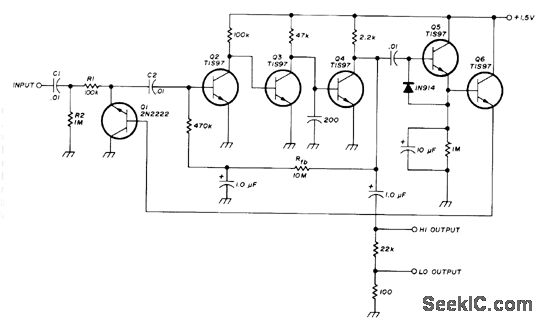
However, then I found the following very interesting circuit that does indeed offer good AGC action and requires only 1.5 volts. I built it in hardware with 1.2 volts and it does work.
The circuit is also visible here: http://www.seekic.com/circuit_diagram/Basic_Circuit/Digital_Circuit/70_dB_GAIN_WITH_15_V.html
I have uploaded an LTspice model of the circuit to https://groups.yahoo.com/neo/groups/regenrx-simulations/files/qrp-gaijin%27s%20files/afamp-agc-hamradio.asc . Note my LTspice model has slightly different component names than in the original circuit. The component names I describe below all refer to the original circuit, not my LTspice model.
It is quite fascinating to look at the techniques used by the circuit designer. In particular:
- The detector transistor Q5 uses an interesting biasing scheme whereby the base bias manages to pull itself up from zero to Vcc over time. A positive peak of the incoming AC AF signal (amplified by Q2/Q3/Q4) slightly turns on the Q5 base. This in turn charges the emitter capacitor. Then, and this is the interesting part, the diode from emitter to base allows that capacitor charge to push up the base bias slightly. Then, the next positive AF peak comes in, again turning on Q5 slightly more, again charging the emitter capacitor slightly more, with this charge again flowing through the diode back to the base, again raising the base voltage slightly. With a high-enough AF signal amplitude (~500 mV), the AF signal will very quickly (in less than 1 second) raise the Q5 emitter and base to the full Vcc potential! With lower AF signal amplitude, the Q5 emitter/base voltage rises more slowly. So the Q5 detector transistor can very quickly generate an AGC control voltage that, for sufficiently large signals, reaches the full Vcc potential.
- Then, the control voltage is taken off of the Q5 detector emitter by the emitter follower Q6, whose emitter load is the Q1 base. The Q1 configuration is also highly interesting. It is an NPN transistor, yet its collector and emitter are reversed; the collector is connected to ground. Q1 appears to be used as a variable resistance, with increasing AGC voltage turning Q1 further on and shunting more of the signal to ground (voltage divider formed by R1/Q1). So, Q1 is being used in saturation mode, but with emitter and collector reversed. As a test in hardware I tried using Q1 the "normal" way with the emitter grounded. The result was motorboating/AF oscillation. With Q1 wired as shown in the circuit, it worked great. LTspice simulations showed that the rate of change of base current is slower when connected as shown in the circuit; when connected "normally" the Q1 base current changes much more rapidly, which presumably causes the motorboating.
The above two transistors (Q1 and Q5) are the most important transistors in the scheme. The AF amp transistors Q2/Q3/Q4 are not so important and can be replaced with another AF amp. I have done exactly this in a prototype on my breadboard now. My prototype circuit uses all 2N3904 transistors and a 1.2-volt supply. (EDIT 2015/09/14: Further LTspice simulation shows that the original DC-coupled AF amp Q2/Q3/Q4 exhibits low distortion and good AGC action even at high signal levels, whereas my own AC-coupled AF amp showed higher distortion and poorer AGC action at high signal levels. It's probably best to stick with the original design's AF amp.)
When testing this circuit with input from the headphone output of a portable transistor radio, adjusting the signal level (volume) on the transistor radio has almost no effect on the amplifier output level, except when the transistor radio's signal level is set to maximum volume, in which case output increases slightly and amplitude clipping distortion is audible. When the signal level is quickly reduced from a high level to a very low level, for the first half second the amplifier output is quiet, then after that the volume rises up as the AGC voltage drops, allowing you to hear the weak signal and the background hiss come up -- just as we would expect from a real AGC.
It was quite interesting to see the circuit design around Q1 and Q5 and to analyse the behavior of Q1 and Q5 in LTspice.
I'm working on a regen now that will incorporate this style of AGC circuit in the AF chain. I think a similar technique could even work to attenuate the RF signal for the AGC loop. However I understand that RF AGC in regens requires careful attention to shielding and signal leakage to prevent undesirable frequency shifts (reference: http://theradioboard.com/rb/viewtopic.php?p=45358#p45358). I'm going to stick with an AF-only AGC for my first experiments.
Update 2015/09/14
Did some more LTspice simulations and hardware testing. As I mentioned in my note above, LTspice simulations showed that the original Q2/Q3/Q4 amp behaved better (in terms of low distortion and good AGC action) than my own ad-hoc amp design. So it seems there was a lot of good engineering that went into the original design.
With this insight, I rebuilt the original AGC circuit as per the above schematic (but still using all 2N3904 transistors). It works fine when hooked up to the headphone output of a a portable transistor radio.
However I ran into problems when I tried to connect it to the output of a 1-transistor regenerative detector (the Vackar-style minimalist detector shown elsewhere on my blog). Volume was very low; the "rushing" sound as the detector transitions into oscillation could barely be heard and was almost in the noise floor.
So, I tried to add a common-emitter preamp and/or a common-collector buffer, but all of my attempts resulted in motorboating and AF oscillation. My usual trick of power supply decoupling (adding a series resistor and large electrolytic capacitor to stabilise the supply voltage for downstream stages) didn't help. More work needed.
Very cool. I prefer AF AGC for regens too -- think of all the complexity that might be needed to make it work for most situations. And also -- you just might add another detector to your circuit!
返信削除I've even used such a circuit as you've described as a driver AGC for a PA -- above a threshold (triggered by poor VSWR on the final) --- more of the driver signal was shunted to ground via a transistor.
Good work!
I think the proble you describe with 2n2904 of less agc action maybe is for the diferences in hfe tis97 has 250~700 and 2904 40~120 thats from datasheets. I dont know exactly but it could be.
返信削除Thanks for pointing out the hfe difference. Maybe I should try to build a version with MPSA18 transistors, which have an hfe between 400 and 1500.
削除