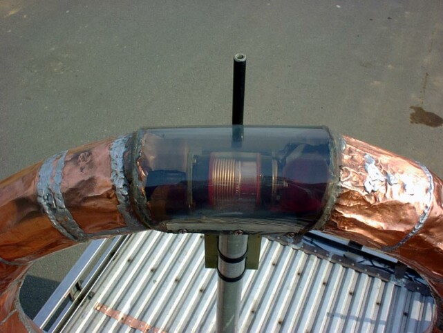
2022年2月11日金曜日

A 1-meter-diameter small transmitting loop for 7 MHz: part 4

Abstract

This post describes the results of Finite-Element-Method simulations (using the software package FEMM) of the RF resistance at 7 MHz of various conductor shapes for use in a small transmitting loop antenna. The conclusion – already known from past theoretical literature, and verified here by simulation – is that a large-diameter, round-cross-section tubular conductor can be replaced with a square-cross-section conductor whose cross-sectional width and height correspond to the tube’s diameter, with negligible change in RF resistance. A new finding is that electrically isolating the four flat faces of the square-cross-section conductor from each other has negligible effect only if the four faces are perfectly aligned to form a perfectly-square cross-section; if, however, the four sides are slightly misaligned to form a distorted approximation of a square, then the RF resistance significantly increases due to uneven distribution among the isolated faces of the RF current which cannot redistribute itself due to the inter-face isolation. Electrically connecting the four flat faces of the square-cross-section conductor may, depending on the conductivity of the connecting material, reduce the RF resistance, by allowing current redistribution and compensating for an imperfect shape of the square cross-section. However, using tin (solder) as a connecting material was found to offer no benefit over leaving the faces disconnected.

Background: Round-cross-section vs. Square-cross-section conductors

As mentioned in a previous post (http://qrp-gaijin.blogspot.com/2017/09/a-1-meter-diameter-small-transmitting.html), H. A. Wheeler’s 1955 article  "Skin Resistance of a Transmission-Line Conductor of Polygon Cross Section" already established that:

If a conductor cross section is any straight-sided polygon that can be circumscribed on a circle, it is found to have the same skin resistance as a conductor whose cross section is this circle. For example, a square wire has the same resistance as a round wire of the same radius, though the square perimeter is 4/pi times as great.
To verify this, a number of Finite-Element-Method computer simulations were performed with the FEMM software.

Analytically computed, the RF resistance Rloss at 7 MHz of a 3.14 meter length (corresponding to a loop antenna of 1 meter diameter) of round copper conductor having 10 cm diameter is 6.81 milliohms, as can be verified by the formulas and calculator at https://chemandy.com/calculators/round-wire-ac-resistance-calculator.htm. The identical result can also be found by assuming an equal current distribution along the entire conductor surface area (as will be the case if the conductor has a round cross-section and is not influenced by the magnetic fields of nearby conductors) and computing the RF sheet resistance of the conductor (https://www.microwaves101.com/encyclopedias/sheet-resistance) using the spreadsheet at https://www.microwaves101.com/uploads/RF-Sheet-Resistance-Rev-7.xls. Using that spreadsheet, the skin depth is computed as 24.60 microns, the surface resistivity per square for a conductor of 5 skin depths thickness is 0.685 milliohms, and for a sheet conductor of 3.14 meters length and 0.314 meters width, the number of squares on that sheet is 10 (3.14m / 0.314m), so the total RF sheet resistance is 10 squares * 0.685 milliohms/square = 6.85 milliohms, which is essentially identical to the previously-computed result of 6.81 milliohms.

Analytically computed, the radiation resistance Rrad of a single-turn, 1 meter diameter loop antenna is approximately 5.7 milliohms, using the approximate formula 31171*(A/lambda^2)^2 (reference:  https://www.ece.mcmaster.ca/faculty/nikolova/antenna_dload/current_lectures/L12_Loop.pdf). Various small-loop calculators also return this same value of radiation resistance for a 1 meter diameter loop (reference: https://owenduffy.net/blog/?p=1693).

Therefore, assuming no other losses, the efficiency is Rrad / (Rrad + Rloss) = 5.7 / (5.7 + 6.85) = ~45%. However, the very low Rrad means that milliohm-level increases in Rloss can have a large effect on efficiency. For example, if Rloss increases by 5 milliohms, then the efficiency drops to 5.7 / (5.7 + 11.85) = ~32%. If Rloss increases by 10 milliohms, the efficiency drops to 5.7 / (5.7 + 16.85) = ~25%.

Given this background, the following FEM simulations were performed.

Simulated RF resistance of a solid, round-cross-section copper conductor

For this first simulation, a solid copper conductor was modeled. FEMM allows modeling a cross-sectional slice of the conductor, which is then effectively rotated about the Z axis to form a loop conductor. The complex impedance of the conductor can be computed at a given frequency, and the real part of the impedance gives the resistive losses. It is also possible to plot the flux density and current density, although this data is not extensively used in this article. We focus mainly on the computed resistive loss at 7 MHz, which includes skin effects and also proximity effects.

Conditions: Mesh resolution was set to 4 microns in a 200-micron-thickness shell at the outer edge of the copper conductor. Higher resolution was not possible due to memory limitations. Mesh resolution was set to automatic (coarser resolution) in the interior of the copper conductor, and in the air region exterior to the conductor. Simulation domain consisted of 3955864 Nodes and 7911456 Elements.

The following image shows the entire simulation domain. The circle in the middle represents the round cross-section of the conductor, which is placed at a distance (radius) of 50 cm from the central vertical axis. The simulation then effectively rotates this cross section around the vertical axis, forming a loop conductor 1 meter in diameter. The several semi-circles at the edge of the problem domain represent the boundary conditions, which were automatically generated by FEMM.

The following images zoom in successively closer to the copper conductor, showing how the problem has been configured with the highest simulation density near the surface of the conductor, to capture skin effects.


Result: RF resistance of 527.96 milliohms was computed. This is an implausible result and is too high. Examination of the simulated current density shows very high current density in the interior of the conductor, which we know analytically to be incorrect. This incorrectly-computed interior current flow, probably computed inaccurately due to the coarse mesh resolution in the interior conductor region, reduces the computed current flow in the outer shell region (which should actually be carrying all of the current), which ultimately leads to a wrong overall current density and a wrong RF resistance value. 

Simulated RF resistance of a hollow, round-cross-section copper conductor

For this next simulation, the interior region of the conductor was replaced with non-conducting air, to prevent any current flow in this region. The only conductive region is the 200-micron copper shell, forming a thin-wall conductor. Since the skin depth at 7 MHz is ~25 microns, the 200-micron shell thickness covers more than 5 skin depths, which is generally considered sufficient for practically minimum RF resistance. 

Conditions: Mesh resolution was set to 5 microns in the 200-micron-thick copper shell. Mesh resolution was set to automatic (coarser resolution) in the air region exterior to the conductor. Simulation domain consisted of 2546258 Nodes and 5092242 Elements.

Result: RF resistance of 7.18 milliohms computed. This is in good agreement with the analytical result of 6.85 milliohms. The RF current is concentrated in the outer-most layers of the thin shell, as expected.

Simulated RF resistance of a thinner-shelled, round-cross-section copper conductor

For this next simulation, the copper shell thickness was reduced from 200 microns to 100 microns. This corresponds to only four skin depths at 7 MHz, not the typically-recommended 5 skin depths.

Conditions: Mesh resolution was set to 3 microns in the 100-micron-thick copper shell. Mesh resolution was set to automatic (coarser resolution) in the air region exterior to the conductor. Simulation domain consisted of 3553075 Nodes and 7105877 Elements.

Result: RF resistance of 7.19 milliohms was computed. This is again in good agreement with the analytical result of 6.85 milliohms. The reduction in shell thickness from 200 microns to 100 microns results in only a negligible change in RF resistance.

Simulated RF resistance of a thin-shelled, almost perfectly square-cross-section copper conductor

For this next simulation, the copper shell shape was changed from round to almost perfectly square. Width was 100.1 mm and height was 100.4 mm. The extra height is to accommodate inserting an isolating air gap between the flat faces, for the next simulation. Shell thickness was 100 microns. To avoid computation errors and unrealistically high current crowding at sharp corners, the 90-degree corners  of the square cross section were changed into rounded curves to smooth out the current flow to more realistic values (since perfectly sharp corners do not exist in physical conductors).

The following image shows the square-cross-section conductor.

The following image shows how the sharp corners of the conductor have been rounded, to avoid simulation anomalies.

Conditions: Mesh resolution was set to 3 microns in the 100-micron-thick copper shell. Mesh resolution was set to automatic (coarser resolution) in the air region exterior to the conductor. Simulation domain consisted of 4601765 Nodes and 9203200 Elements.

Result: RF resistance of 7.09 milliohms was computed. The change of conductor cross section from round to square results in only a negligible change in RF resistance. The value is still in good agreement with the analytical result of 6.85 milliohms.

Simulated RF resistance of a thin-shelled, almost perfectly square-cross-section copper conductor with isolated walls

For this next simulation, the four faces or walls of the square-cross-section conductor were disconnected from each other by inserting small air gaps at each corner. Because the current ideally should flow longitudinally along each face and along the circumference of the loop, the air gaps – which are in line with the current flow – should theoretically not hinder the current flow and should not change the RF resistance. The air gaps only prevent the current from flowing cross-wise from one face to another adjoining face. However, normally we would expect that current need not flow cross-wise from one face to another face.

Conditions: Mesh resolution was set to 3 microns in the 100-micron-thick copper shell. Mesh resolution was set to automatic (coarser resolution) in the air region exterior to the conductor. Simulation domain consisted of 4595785 Nodes and 9191231 Elements.

The following image shows how an air gap has been inserted between adjoining sides of the square-cross-section conductor.

Result: RF resistance of 7.27 milliohms was computed. The change of isolating the adjoining conductor faces by insertion of air gaps (in line with the direction of the current flow) results in only a negligible change in RF resistance. The value is still in good agreement with the analytical result of 6.85 milliohms.

Simulated RF resistance of a thin-shelled, distorted square-cross-section copper conductor with isolated walls

For this next simulation, the four isolated faces or walls of the square-cross-section conductor were distorted from the perfect square shape by randomly moving each end of each edge by a few millimeters in the x and y directions. A real physical construction of such a square-cross-section conductor may have small imperfections in the square cross-sectional shape, and the purpose of this simulation was to see if these imperfections would cause an increase in RF resistance.

Conditions: Mesh resolution was set to 3 microns in the 100-micron-thick copper shell. Mesh resolution was set to automatic (coarser resolution) in the air region exterior to the conductor. Simulation domain consisted of 4521864 Nodes and 9043451 Elements.

The following image shows the distorted, approximately-square cross-section of the conductor, with the adjacent sides still disconnected by an air gap.

Result: RF resistance of 12.27 milliohms was computed. This is a significant increase in RF resistance. A perfectly square cross-sectional shape leads to perfectly balanced current distribution among four faces, even if those faces are electrically isolated from one another. However, a distorted cross-sectional shape leads to a poorer current distribution among the faces, which, due to the inter-face isolation, can no longer redistribute itself more evenly among the faces. The resulting poor current distribution reduces the amount of the conductor that is used to carry current, hence increasing the RF resistance.

Simulated RF resistance of a thin-shelled, distorted square-cross-section copper conductor with thin copper connectors between adjoining walls

For this next simulation, the isolated faces of the distorted square-cross-section conductor were connected with each other. The hope is that by electrically connecting the isolated and misaligned faces, the poor current distribution – caused by the distorted shape and misaligned faces – can somewhat balance itself out again if the current is allowed to flow cross-wise from one misaligned face onto an adjoining misaligned face. The air gaps between the corners of the faces were bridged with a copper conductor. Again, sharp edges were changed to round edges to prevent simulation anomalies. 

Conditions: Mesh resolution was set to 3 microns in the 100-micron-thick copper shell. Mesh resolution was set to automatic (coarser resolution) in the air region exterior to the conductor. Simulation domain consisted of 4824805 Nodes and 9649327 Elements.

The following image shows how the air gaps at the corners of the misaligned sides have been bridged with a copper conductor.


Result: RF resistance of 8.12 milliohms was computed. This is lower than the 12.27 milliohms of the distorted conductor with disconnected faces. Therefore, we can conclude that connecting the misaligned faces to allow cross-wise current flow between adjacent misaligned faces does improve the current distribution and does reduce the RF resistance. However, the resulting RF resistance of this misaligned and connected square-cross-section conductor is still higher than the 7.09 milliohms of the perfectly-aligned and connected square-cross-sectional conductor. So even with inter-face connections, the distortion of the cross-sectional shape still has a small, detrimental effect on the RF resistance.

Simulated RF resistance of a thin-shelled, distorted square-cross-section copper conductor with thin stainless steel connectors between adjoining walls

For this next simulation, the copper conductors that bridge the gaps between the misaligned faces were replaced with stainless steel conductors. The background to this idea is that in a physical construction of a square-cross-section conductor, the four flat faces (flat sheets of copper) can be laid separately on the outside of a square-cross-section plastic tube. This leaves four air gaps at the corners, with each gap running along the length of the square tube, and with each gap separating the the edges of two adjoining flat copper sheets. These air gaps can then be soldered for electrical connectivity. However, the electrical resistance of solder is higher than that of copper. For simulation purposes, it could be appropriate to use tin as a conductor to simulate the higher resistance of solder. However, the FEMM software does not offer tin as part of its material library. As a subsitute, 304 stainless steel (which is provided with the default FEMM material library, with conductivity specified as 1.45 MS/m) was used as a connecting material in the simulation. Steel has a much higher resistance than copper or tin, and so should provide an upper bound on the RF resistance. The expectation was that since the connecting material’s area is so small compared to the main copper conductors’ area, the impact on RF resistance should be negligible. 

Conditions: Mesh resolution was set to 3 microns in the 100-micron-thick copper shell. Mesh resolution was set to automatic (coarser resolution) in the air region exterior to the conductor. Simulation domain consisted of 4825265 Nodes and 9650247 Elements.

The following image shows how the connecting corner conductor, that bridges the gap between the misaligned vertical conductor and misaligned horizontal conductor, has been changed to a steel conductor, while the main conducting areas are still configured as copper.


Result: RF resistance of 32.41 milliohms was computed. This is contrary to expectation and seems unusually high. Introducing the stainless steel connectors has actually increased the RF resistance far above the RF resistance that occurs when the faces are left unconnected. The presence of stainless steel seems to be worse than no connection at all.

Examination of the current density showed extremely high current concentration in the stainless steel regions. The cause appeared to be the insufficient thickness (100 microns) of the stainless steel conductor. 100 micron thickness covers 4 skin depths of copper at 7 MHz, but it covers less than 1 skin depth in stainless steel at 7 MHz, because the skin depth of stainless steel at 7 MHz is approximately 161 microns. To cover 5 skin depths in stainless steel requires approximately 805 microns of thickness, so another simulation was run with thicker stainless steel connectors.

Simulated RF resistance of a thin-shelled, distorted square-cross-section copper conductor with thick stainless steel connectors between adjoining walls

For this next simulation, the thickness of the conductor thickness in the stainless steel connecting areas was increased to approximately 900 microns, to cover 5 skin depths in stainless steel at 7 MHz. After thickening the connectors, the sharp corners were rounded. Copper conductors were left at 100 microns thickness. The expectation was that the current flow in the steel areas should be essentially maximal, due to the 5-skin-depth thickness, and that the overall impact on RF resistance should be small, since the circumferential length (around the conductor’s cross-sectional perimeter) occupied by the steel connectors is small compared to the circumferential length occupied by the copper conducting surfaces.

Conditions: Mesh resolution was set to 3 microns in the 100-micron-thick copper shell. Mesh resolution was set to 30 microns in the approximately 900-micron-thick stainless steel connecting areas, to encompass 4 to 5 skin depths of stainless steel at 7 MHz. Mesh resolution was set to automatic (coarser resolution) in the air region exterior to the conductor. Simulation domain consisted of 4825560 Nodes and 9063542 Elements.

Results: RF resistance of 29.65 milliohms was computed. This is only a small improvement over the previous RF resistance (with thinner steel connectors) of 32.41 milliohms. Therefore, the thickness of the stainless steel connectors does not seem to be the primary cause of the increased RF resistance.

One explanation may be that the very presence of the stainless steel itself is causing the increased RF resistance. An anecdotal report that stainless steel greatly increases RF resistance can be found here: https://www.eham.net/community/smf/index.php/topic,83113.0.html.

Another alternative explanation may be that the simulation resolution in the stainless steel area (30 microns) is too coarse to compute an accurate resistance. It is not possible, in the above simulation, to increase the simulation resolution in the thick stainless steel areas, because then the mesh size exceeds the available memory. To investigate this hypothesis further, it should be possible to run a separate simulation with a thin-shelled (5 skin depths) stainless steel conductor, once with 3 micron resolution, and once with 30 micron resolution. The mesh size can be minimized to fit within available memory by reducing the conductor diameter as necessary. Then, the RF resistance can be compared between the 3-micron-resolution run and the 30-micron-resolution run. If the computed RF resistance is significantly different, this indicates that a 30-micron resolution is too coarse.

Simulated RF resistance of a thin-shelled, distorted square-cross-section copper conductor with thin aluminum connectors between adjoining walls

For this next simulation, the connecting areas were changed from stainless steel to aluminum (which is provided with the default FEMM material library, with conductivity specified as 24.59 MS/m). The problem geometry was copied from the previous test case with thin copper connectors, meaning that all conductors and connectors were set to 100 micron thickness and sharp corners were rounded in the same way as in the previous test case with thin copper connectors. 100 micron thickness should be enough to cover 3 skin depths in aluminum at 7 MHz.

Conditions: Mesh resolution was set to 3 microns in the 100-micron-thick copper shell and in the 100-micron-thick aluminum connectors. Mesh resolution was set to automatic (coarser resolution) in the air region exterior to the conductor. Simulation domain consisted of 4825560 Nodes and 9650835 Elements.

Result: RF resistance of 9.71 milliohms was computed. This is higher than the 8.12 milliohms RF resistance when using thin copper connectors, but lower than the 29.65 milliohms RF resistance when using thick stainless steel connectors. It is also lower than the 12.27 milliohms RF resistance when the faces are disconnected from one another.


Simulated RF resistance of a thin-shelled, distorted square-cross-section copper conductor with thin tin connectors between adjoining walls

For this next simulation, the connecting areas were changed from aluminum to tin, to simulate the resistance of ordinary solder. The FEMM default material library does not provide a tin material. Examination of other default FEMM material library entries for copper, aluminum, and stainless steel revealed that the only parameter that is necessary to define a new material is the material's conductivity in MS/m. The conductivity of tin is 8.7 MS/m, and a new FEMM material was created with this conductivity, leaving all other material parameters as-is. The problem geometry was copied from the previous test case with thin copper connectors, meaning that all conductors and connectors were set to 100 micron thickness and sharp corners were rounded in the same way as in the previous test case with thin copper connectors. A 100 micron thickness covers slightly more than one skin depth (64.49 microns) of tin at 7 MHz.

Conditions: Mesh resolution was set to 3 microns in the 100-micron-thick copper shell and in the 100-micron-thick tin connectors. Mesh resolution was set to automatic (coarser resolution) in the air region exterior to the conductor. Simulation domain consisted of 4825560 Nodes and 9650835 Elements.

Result: RF resistance of 12.84 milliohms was computed. This is higher than the RF resistance when using copper or aluminum connectors, but is lower than the RF resistance when using thick stainless steel connectors. However,  the RF resistance is actually higher than the 12.27 milliohms obtained when the faces are disconnected from one another. Even higher total RF resistance would be expected if the resistivity of the solder is actually higher than that of tin,as for example shown in the resistivity table at https://owenduffy.net/antenna/conductors/loss.htm

Summary of simulated RF resistance values

The following FEM simulation results were obtained for the RF resistance of a 10 cm diameter conductor of various configurations. These should be compared with the analytical result of 6.85 milliohms RF resistance at 7 MHz for a solid round conductor with 10 cm diameter. 

  • Solid 10 cm round conductor: 527.96 milliohms (wrong result)
  • Hollow 10 cm round conductor with 200 micron shell: 7.18 milliohms
  • Hollow 10 cm round conductor with 100 micron shell: 7.19 milliohms
  • Hollow 10 cm square conductor with 100 micron shell: 7.09 milliohms
  • Hollow 10 cm square conductor with disconnected 100 micron shell: 7.27 milliohms
  • Hollow 10 cm square conductor with disconnected and misaligned 100 micron shell: 12.27 milliohms
  • Hollow 10 cm square conductor with misaligned 100 micron shell connected by thin copper connectors: 8.12 milliohms
  • Hollow 10 cm square conductor with misaligned 100 micron shell connected by thin stainless steel connectors: 32.41 milliohms
  • Hollow 10 cm square conductor with misaligned 100 micron shell connected by thick stainless steel connectors: 29.65 milliohms
  • Hollow 10 cm square conductor with misaligned 100 micron shell connected by thin aluminum connectors: 9.71 milliohms 
  • Hollow 10 cm square conductor with misaligned 100 micron shell connected by thin tin connectors: 12.84 milliohms

Conclusions

For a 1-meter-diameter loop antenna at 7 MHz, the low radiation resistance of 5.7 milliohms requires a correspondingly low-loss conductor to achieve reasonable efficiency. With a 10 cm diameter conductor, a square-cross-section conductor – which in some respects is easier to fabricate than a round-cross-section conductor – can provide sufficiently low RF resistance.

However, small details of the conductor geometry can cause significant changes in the overall RF resistance. This is important because fabricating a 10 cm-wide square-cross-section conductor by hand, by separately assembling several flat sheets of copper, will inevitably lead to small misalignment among the faces and distortions from the ideal, perfectly-shaped, square cross-section.

If the flat sides of the square cross-section conductor are galvanically isolated from one another, then small misalignment, on the order of a few millimeters, of the flat sides of the square-cross-section conductor can lead to significant increases of RF resistance.

If the misaligned flat sides of the square-cross-section conductor are connected to each other with copper, the RF resistance decreases to acceptable levels (only slightly above that of the perfectly-aligned case) because the current is allowed to flow cross-wise from one misaligned face to an adjoining misaligned face, which will improve current distribution and reduce the conductor’s RF resistance.

However, if the misaligned flat sides of the square-cross-section conductor are connected to each other with low-conductivity stainless steel, the RF resistance significantly increases to unacceptably high levels -- higher than if the faces were left unconnected.

If an aluminum conductor is used to connect the misaligned flat sides, then the RF resistance lies between that of copper connectors and that of stainless steel connectors.

If a tin conductor is used to connect the misaligned flat sides, then the RF resistance is comparably high to the case where the flat sides are left disconnected.

Therefore, the material used to connect the misaligned flat sides of the square-cross-section conductor will have an influence on the overall RF resistance. In practice, tin solder, with a resistivity similar to that of tin, will be the most likely material used to connect the faces. In the above simulations, using tin solder to connect misaligned faces was found to have no benefit over leaving the misaligned faces disconnected

Further studies with varying amounts of misalignment would be needed to clarify whether there are any cases where soldering misaligned faces would bring any benefit, but the current results suggest there will be minimal, if any, benefit. 

A likely more beneficial strategy would consist of two points. First, attempt to avoid misalignment of the cross-sectional shape from a perfect square or perfect circle; this can be done with a rigid former and/or with thick copper that is less subject to deformation, but both of these measures increase the weight and the difficulty of working with the materials. Second, avoid separating the faces in the first place, by avoiding the use of four separate copper sheets to form four separated flat faces of one tube, and instead rolling a continuous copper sheet into a large-diameter tube. This again is more difficult to construct (since a single and large copper sheet must be rolled to yield a perfectly circular or square cross-sectional shape), but likely will yield the lowest RF resistance for the conductor. This roll-up construction would still leave one unconnected seam along the tube's length. The effect of this seam is likely minimal, but a simulation should be performed to confirm this.

2021年3月28日日曜日

3D printing, self-repair, and self-replication: RepRap


 A "RepRap" 3D printer is a pretty amazing thing. Nowadays, 3D printers are widely and cheaply available, but ten years ago, this was not the case. One of the driving forces behind the advances in consumer-level 3D printing has been the RepRap project at https://reprap.org.

A RepRep machine is a rapid prototyping machine that can manufacture a significant portion of its own parts. This means that a RepRap printer can, to a large extent, repair itself, by printing new plastic parts to replace its own plastic parts, such as gears, that can wear out over time. Similarly, a RepRap 3D printer can, to a large extent, replicate itself, by printing out all of the plastic parts needed to build another copy of the printer. In contrast, modern 3D printers, in their quest for compactness and reliability, have moved away from the self-replicating aspect of the RepRap vision. Modern 3D printers use many custom-manufactured parts (such as smaller, more precise, and more reliable gears, or custom-molded metal structural parts), that cannot be printed by the 3D printer itself. The result is higher reliability, smaller size, lower cost, and improved user-friendliness.

So modern 3D printers are closer to black-box appliances that are not designed for extensive user maintenance and modification. In stark contrast, a RepRap machine at its core not only allows, but also requires extensive maintenance and modification by the user. RepRap printers are therefore less user-friendly as appliances, but they also offer endless opportunity for modification and improvement.

A RepRap 3D printer can be a very fun hobby for a DIY-minded person, so I plan to describe my adventures in 3D printing here on my blog.

Nine years ago: the Portabee 3D printer

Nine years ago, the company Romscraj released the Portabee 3D printer: https://reprap.org/forum/read.php?188,133194,133194#msg-133194 . Its key sales point was its portability: the print bed could be detached or reattached in seconds with a clever clip mechanism. In the detached state, the entire printer could fit inside of a laptop bag. And this printer was a RepRap, meaning it could reproduce all of its own plastic parts, making it easy to build another copy of the printer, or to improve the original printer design. After reading several positive reviews about the Portabee, I bought the printer.

There is a Wiki page at https://reprap.org/wiki/Portabee, where I am trying to collect all relevant information about this interesting little 3D printer.

I didn't have much time to use the Portabee after I purchased it, so it sat idle for several years. Only recently have I started to use it heavily.

Fast forward nine years: a printer in need of maintenance

One of the problems I immediately encountered with the Portabee was that the 3D-printed plastic gears on the extruder -- the geared mechanism that uses a stepper motor to push plastic filament into the hot end, where it gets melted and extruded out of a thin nozzle -- were prone to breaking. Within one month of the original purchase, the first plastic drive gear broke, and the supplier provided me with a replacement.

Now, nine years later, when I was powering up the printer again, I could see that the plastic extruder gears did not fit together perfectly, which caused undue stress on the gears. Every time I operated the printer, bits of the plastic drive gear would break off, leaving small chips of broken plastic on the print bed. I could tell that it was only a matter of time before the gears broke again.

The solution, of course, is to use the 3D printer to print replacement parts for itself. The problem was that I was still a novice to 3D printing. My first attempts to print the replacement drive gear came out horribly deformed. Below, the left gear in blue is the original broken gear from 9 years ago. The right two gears were my first attempts at printing replacements.

I quickly learned that effective use of a 3D printer requires understanding at least the fundamentals of the physical processes being used. In this case, by observing the printer in operation, I could see that when printing the small and detailed teeth of the gear, the lower layers of plastic did not have enough time to cool before the next layer of molten plastic was deposited on top of them. The result was overheating and a mess of molten plastic where the gear teeth should have been.

There are many ways to solve this problem:

  1. Use a cooling fan to blow air over the printed part and cause the molten plastic to cool more quickly. I didn't have a cooling fan, so this was not an option.

  2. Greatly reduce the print speed. In practice, this resulted in too little plastic being extruded and very fragile appearance of the gear teeth. Probably, at extremely slow printing speeds, the gears' movement is not accurate enough to ensure a constant flow of molten plastic filament.

    Imagine trying to squeeze toothpaste out of the tube at a rate of 1 cm/second. This is feasible with a good flow rate. On the other hand, if you try to greatly reduce the extrusion rate by a factor of 100, you would need to squeeze toothpaste out at a rate of 0.1 mm/second. This is extremely difficult, because even slightly inaccurate movements of your hands, or even slight deformations of the tube, will cause unwanted variations in the flow rate. I suspect a similar issue occurs at extremely slow print speeds.

  3. Print at full speed, but print multiple copies of the gear on the print bed. All copies are built up simultaneously from the lowest Z-layer to the highest Z-layer. This means that each Z-layer takes more time to print. This increased printing time allows each individual copy of the gear to cool down enough before the next layer of plastic is laid on top of it.

    The disadvantage of this approach is that, when moving the hot nozzle from one printed item to another, a so-called "retraction" is performed, which reverses the motion of the extruder gears to withdraw the plastic filament from the nozzle and prevent unwanted oozing of molten plastic.

    The use of retraction (due to the rapid reversal of motor direction) caused visibly more wear on my already-disintegrating drive gear. Furthermore, after a retraction, the next act of extruding filament may not extrude enough, which leads again to fragile-looking gear teeth with insufficient plastic material. This might be fixed by adjusting retraction parameters in software.

  4. Print the gear at full speed, but at the same time print a very tall cylindrical wall (a "skirt") around the gear, some distance away from the gear. For each layer, after the small gear teeth are printed, then during the printing of the long cylindrical wall, the small gear teeth have time to cool, before the next layer of molten plastic is printed on top of them.

    This approach used fewer retractions, resulting in less stress on the motor gears, better flow of plastic, and an overall improved and sturdy appearance of the gear teeth.

The self-repairing printer

Shortly after figuring out how to successfully print good-looking replacement gears, the drive gear again broke. So I was forced to replace the original gear with the self-printed replacement. I was hesitant and unsure if the printed replacement would really fit and would really work properly.

Fortunately, it did fit, well enough to keep the printer running. 

Here's a picture of the original extruder. The weak drive gear, printed 9 years ago by the manufacturer when I bought the printer, is the smaller 9-tooth gear attached to the motor.

Then, one day soon thereafter, the drive gear broke:


The key to a self-repairing 3D printer is to print enough replacement parts before the printer breaks. Here were the as of yet untested replacement parts that I was able to print before the breakage.

The holes in the replacement parts unfortunately were a bit too small to fit the motor shaft -- a common problem in 3D printing. This was fixed by reaming the hole with a screwdriver, as I don't have a proper reamer. After that, I was able to fit the replacement drive gear on the motor shaft.

Then, I could confirm that the replacement drive gear more-or-less meshed correctly with the larger 53-tooth driven gear.

After the gear replacement, the printer could again print. The first self-repair was successful!

Other self-repairs: broken extruder block, broken driven gear

Soon thereafter, the extruder block -- the complex-shaped part that holds the extruder motor and drives the filament forward -- also broke. The long arm that supports the motor had become warped and finally cracked. I suspect that this warping was one of the root causes of why the drive gear and driven gear did not mesh well, which caused the drive gear to weaken and break.

The design of the extruder block (see image below) uses a fairly thin and long support arm to hold the extruder motor in place. The extruder motor may become hot, as it is in constant motion during a print to feed the filament. If the heat from the motor becomes excessive, this heat may cause the plastic support arm on the extruder block to soften and warp, which in turn can cause the gear alignment to suffer, which in turn can cause inappropriate stress on the extruder gears and on the extruder block itself.

I didn't have a replacement extruder block, as I hadn't printed one yet. So, I had to repair the cracked extruder block with some super-glue. I used rubber bands to hold the part together tightly, and allowed the glued part to dry overnight. Fortunately, this worked well enough, and the next day I could then print a replacement extruder block.

The below image shows the original extruder block (left), and the new printed replacement (right).

Finally, a few days after replacing the extruder block, the large 53-tooth driven gear also broke. Fortunately, I had already predicted this scenario, and had already printed several replacements.

Here is an image of the new extruder in action: most of the original extruder parts (originally printed in blue plastic) have been replaced with new, self-printed parts (now printed in white plastic). Also, the below images shows even more replacement parts being printed, in preparation for the next time that these high-usage parts break.

Replacing the heating element

Recently, the hot end has no longer been able to reach the high temperatures (185 degrees) required for melting the plastic filament. I suspect that the heating element is no longer able to heat up properly, since it is 9 years old. 

Modern ceramic heating elements seems to be easily available in a standardized 6 mm-diameter size. However, the hole in my heater block only seems to accommodate a heating element of less than 5 mm diameter. The current heating element is a wire-wound resistor. Due to the size difference, I probably cannot use a modern 6 mm ceramic heater, and instead need to find a less than 5 mm diameter wire-wound resistor.

Replacing the hot end 

Eventually, I will need to replace the hot end completely, because it accepts 3 mm diameter plastic filament, which was a widespread standard 9 years ago. Now, most filaments are available in 1.75 mm diameter, so I will need to upgrade to a new 1.75 mm hot end when my old supply of 3 mm diameter filament runs out.

This will require reworking the mounting mechanics for the hot end, as the new hot end will be a different shape than the old hot end. Reworking the mechanics will be done, of course, by using the printer itself to print new parts in the appropriate redesigned shapes. This again underscores the self-repairing, self-modifying nature of RepRap 3D printers.

Replacing the electronics board

Recently, the printer has sometimes been acting strangely, after the electronics board was exposed to rain. Sometimes, the Y-axis motor (which slides the printed bed back and forth) only buzzes instead of properly moving the bed. I could trace this fault to an unusually low Vref voltage on the DRV8811 driver chip that drives the Y-axis stepper motor. In modern 3D printer control boards, often the driver chips are modular so they can be replaced easily by unplugging the old driver and plugging in a new driver. In my old electronics board (a so-called gen6.d board that came with the Portabee printer), the motor driver chips are soldered onto the board itself and cannot be replaced without replacing the whole board.

It turns out that the exact gen6.d board used in my Portabee printer is no longer available for purchase, at least as far as I could see. But fortunately, control boards for 3D printers are quite standardized these days and are available cheaply. The basic options are either a RAMPS 1.4 board plus a controlling Arduino board (a 2-board solution), or an all-in-one single-board solution like an MKS GEN board, which I think uses the same basic architecture, just packaged more neatly into a single board. Either solution provides connectors for controlling five stepper motors (three for each of the X, Y, and Z axes, and up to two extruder motors), limit switches for each of the axes, the hot end (including the heating element, the thermistor to detect the temperature, and a cooling fan), and a heated bed (including the heater and the thermistor). 

Carefully checking all of the connections on my Portabee has convinced me that a modern replacement board (like RAMPS 1.4 or MKS GEN) will provide all the required connectors to control all of the hardware on my Portabee printer. The only exception is that I have 2 Z-axis motors, whereas most controller boards only provide one connector for a Z-axis motor -- but two Z-axis motors can be connected either in parallel or in series to a single connector.

The below image shows the old gen6.d control board connected to all of the 3D printer hardware.

The below image shows the old gen6.d control board disconnected from all of the printer hardware.

Disconnected from the controller board, the printer somehow seems much simpler -- it's just a bunch of stepper motors, switches, heaters, and thermistors, all tied together into a simple but sturdy physical structure with 3D-printed parts and common hardware like steel rods, threaded rods, linear bearings, nuts, bolts, belts, etc.

To replace the electronics, the only thing left to do is to buy a new replacement board, and plug all the existing hardware into the new replacement board. Some caution will be required with the order of the stepper motor wires, as modern control boards seem to require the stepper wires to be connected in a different order than on my older control board. I may also need to make some of the wires slightly longer to accommodate the new connector positions on the new control board.

Conclusion

Out of necessity, I have been replacing many parts of my old 3D printer, with self-printed replacement parts. This is an educational and fun experience. Eventually, I should have enough spare parts and enough knowledge to build a complete replica of the original printer. And I expect to continue to improve the printer design by printing out modified, improved parts, to accommodate for example a new hot end.

2020年10月10日土曜日

A sensitive, frequency-modulated dip meter capable of measuring resonator Q

Abstract

A highly-sensitive, narrow-band frequency-modulated dip meter offers a simple way to measure resonator Q.

Background

I have been working with an unusual dip meter circuit recently that has some interesting properties.

The dip meter, also called a grid dip meter, is a simple homebrew instrument that offers a wide range of measurement possibilities. For an introduction to dip meters, please see https://hackaday.com/2015/11/30/the-grid-dip-meter-forgotten-instrument/ and https://www.robkalmeijer.nl/techniek/electronica/radiotechniek/hambladen/qst/2002/05/page65/index.html .

Problem with existing dip meters: low sensitivity

The problem with most dip meters is low sensitivity. A strong magnetic coupling to the device under test is required to obtain a sufficiently-large dip to be noticed. On the other hand, strong coupling has the disadvantage that it detunes the oscillator and also loads the device under test, reducing its Q. 

Ideally, the coupling should be as weak as possible to obtain the most accurate result. But with weak coupling, the meter deflection is very small and very difficult to discern.

As an example of low dip meter sensitivity, see the following video. This is a simple and traditional dip meter (GDO), dipping a ferrite rod antenna. A weak dip of a few microamps can be detected. The circuitry surrounding the ferrite rod forms a superheterodyne receiver, which is turned off and is irrelevant for this test. At the end of the video, after the dip is detected, I move the dip meter physically farther from and closer to the coil, to indicate how the dip meter output changes with distance to the coil being dipped. 

https://www.youtube.com/watch?v=iK8aZhySox8


The dip is very small, and the movement of the needle is very difficult to discern on the meter.

The circuit for this dip meter is from the webpage of Mr. B. Kainka at http://www.b-kainka.de/bastel53.htm. The signal that moves the meter is a DC signal derived from the RF oscillator's voltage. Because this is a DC signal, it is more complicated to amplify than an AC signal.

Improved dip meter sensitivity: Narrow-band frequency modulation generates easy-to-amplify AC signal

One good solution to improving dip meter sensitivity is to introduce a small frequency modulation onto the dip meter's RF oscillator. The dip meter frequency repeatedly is swept up and down by several kHz around the currently-tuned frequency of the dip meter. The sweep frequency is at an audio frequency such as 500 Hz.

This repeated, narrow-band frequency modulation then generates a small 500 Hz AC signal that corresponds to the variation in oscillator amplitude inside of the narrow-band sweep. If the oscillator amplitude does not vary, or varies only slightly, inside of this few-kHz sweep width, then no signal or only a very small AC signal is generated. On the other hand, if the oscillator amplitude starts to change rapidly inside of the few-kHz sweep width -- as will be the case when the dip meter is tuned to a frequency where a dip is present -- then a large 500 Hz AC signal is generated. What is actually happening is that we are measuring the rate of change of the resonance curve of the device under test. The greater the rate of change, the greater the oscillator amplitude variation inside of the repeating narrow-band frequency sweep, and the greater the amplitude of the generated 500 Hz AC signal.

The generated 500 Hz AC signal -- since it is AC and not DC -- can then easily be amplified by a normal AF amplifier such as an LM386. The amplified audio signal can then be monitored directly via headphones, and can also be used to drive a meter or an LED for visual display.

To my knowledge, the first and only commercial dip meter to use this concept is the DipIt meter, described here: https://www.qrpproject.de/UK/DipItUk.html. (Edited 2024/07 -- link seems dead; here is an alternative link: https://www.qsl.net/sp5btb/DipIt.pdf .)

However, the concept of frequency-modulating the dip meter is not new. As far back as 1972, the technique was already fully described within the context of nuclear quadropole resonance experiments by M. Suhara at http://scirep.w3.kanazawa-u.ac.jp/articles/17-01-002.pdf

Quote (emphasis added):

In  magnetic resonance experiment,the nuclear signal can be detected through modulations; one is frequency modulation and other magnetic field modulation (or Zeeman modulation). In principle, the use of frequency modulation of the source oscillator of a radio-frequency spectrometer offers an attractive mode of operation. As the frequency of the spectrometer oscillator moves back and forth in the region of an absorption line of the sample, the latter produces amplitude modulation, which can be observed by means of an amplitude detector, followed by narrow-band amplification and phase-sensitive detection at the modulation frequency.

Because the frequency-modulation technique was already fully-described in 1972, it is likely that the technique was already known several years earlier.

My frequency-modulated dip meter circuit

My dip meter circuit is as follows.


The principle of operation is described on the schematic image and requires no further explanation here.

Here is a video of my frequency-modulated dip meter in use.

https://www.youtube.com/watch?v=nVi3L0BwaXg

In the above video, the new, frequency-modulated dip meter is used to detect a dip in the same configuration as the previous video with the traditional (non-frequency-modulated) dip meter. The new circuit clearly shows much better sensitivity. A strong dip is indicated by a loud audio tone and bright LED illumination. At the end of the video, after the dip is detected, I move the dip meter physically farther from and closer to the coil, to indicate how the dip meter outputs (audio volume and LED brightness) change with distance to the coil being dipped.

Measuring Q with a traditional (non-frequency-modulated) dip meter

It is probably well-known that a dip meter can be used to measure Q of an inductor or resonant tank. See for instance https://www.robkalmeijer.nl/techniek/electronica/radiotechniek/hambladen/qst/2002/05/page65/index.html. You essentially tune the dip meter for a deep dip, then slowly tune the meter to either side of the dip until the dip depth is reduced by 30%, that is, such that the dip is only 70% of its original value. Then, the frequency difference between the two 70%-dip frequencies is the -3 dB bandwidth. In other words, as the oscillator is tuned across the dip, the dip in oscillator amplitude basically follows the shape of the resonance curve of the device under test.

This method is already attractive because it requires no direct connection to the device under test. But the problem with this approach is that it requires a rather high level of inductive coupling to the resonator to get a deep dip. Such high coupling can cause unwanted loading of the device under test. Also, it is difficult and tedious to identify, from meter readings, when the meter value corresponds to 70% of its maximum deflection from the baseline value. It is even more difficult when the coupling is reduced to a minimum, which also then reduces the meter deflection to a minimum.

Measuring Q with a narrow-band frequency-modulated dip meter

It was mentioned above that with a narrow-band frequency-modulated dip meter, we are not measuring the resonator response of the device under test, but instead we are measuring the rate of change -- the first derivative -- of the resonator response.

Therefore, when manually tuning a narrow-band frequency-modulated dip meter across the resonance frequency of a resonator being tested, you get a null (a zero rate of change) at the exact center resonance frequency. You also get two peaks, one on each side of the resonance frequency -- these peaks correspond to the frequencies where the slope (the rate of change of the resonance curve) is maximum.

It turns out that at the frequencies where these two peaks occur -- at the frequencies where the slope of the resonance curve is maximum -- the amplitude of the resonance curve has dropped to 75%. This is proved by finding the zero-crossing points of the second derivative of a Cauchy-Lorentz function that mathematically models the resonance response (see https://en.wikipedia.org/wiki/Cauchy_distribution). I plan to write a summary of the derivation and post it here on my blog in the future, but the basic idea is that the zero-crossings of the second derivative show the location of the maximum/minimum points of the first derivative (and the first derivative is what we measure with the frequency-modulated dip meter). If we take the algebraic expressions for frequencies where these second-derivative zero-crossings occur, and use those frequencies to evaluate the value of the original Cauchy-Lorentz function (the resonance response function) in relation to the maximum value of the Cauchy-Lorentz function, it turns out that the relationship is that the value is always 75% of the maximum value.

In other words, the frequency difference between the dual peaks that are measured on a narrow-band frequency-modulated dip meter corresponds to a bandwidth where the resonator response has reduced to 75% of its maximum. This corresponds to a -2.498 dB bandwidth, which can (with some more pages of mathematical derivation) be converted to a -3 dB bandwidth by multiplying by a scaling factor of 1.1147.

Below is an image showing a resonance curve, its first derivative, and the absolute value of its first derivative (lower right). The lower-right image corresponds to the output data that would be obtained from a narrow-band frequency-modulated dip meter that is tuned across the resonance peak of a device under test.


Conclusion

This new kind of dip meter -- a narrow-band frequency-modulated dip meter that measures the first derivative of the resonance curve, and that generates an AC output signal that can be easily amplified and thus leads to good sensitivity -- potentially offers an easy way to measure resonator bandwidth (and hence Q) with minimal loading of the device under test. All that is needed is some quite light magnetic coupling to the inductor under test.

The special thing about the new kind of narrow-band frequency-modulated dip meter is that its sensitivity is increased, and it offers two unambiguous peaks that serve as "markers" of where the resonator response has dropped to 75% of its maximum. This should make bandwidth measurement easier as compared with traditional (non-frequency-modulated) dip meters.

I should add that I am not an expert on Q measurements, but I am very intrigued by the ability of this new dip meter design to fairly easily measure inductor Q. I do not have other test equipment capable of measuring resonator Q, but I hope that some other experimenters with better test equipment might be encouraged to build this kind of a new dip meter and to compare the bandwidth and Q measurements from the dip meter (bandwidth = 1.1147 * frequency difference between the two peaks; then Q=frequency/bandwidth) with the Q measurements obtained by other means.

Of course, the whole idea of using a dip meter to measure resonator bandwidth is quaint and outdated in this day and age of $50 vector network analysers. But it's much more fun and educational (for me anyway) to use traditional and hands-on methods, instead of punching some buttons and reading the result from a computer screen.

2018年10月7日日曜日

A 1-meter-diameter small transmitting loop for 7 MHz: part 3

This post considers some practical aspects of capacitor mounting, in order to connect the vacuum variable capacitor with minimum loss to the 10 cm^2-cross-section loop conductor.

Disadvantages of vertical capacitor mounting


The previous post in this series (part 2) considered two mountings of the vacuum variable capacitor, a vertical mounting and a horizontal mounting. Previously, I had concluded that "for mechanical simplicity, likely the variable capacitor will/must be mounted in the vertical position for this project," as shown in the below diagram.


Schematically this vertical capacitor mounting would look as follows.


However, as noted in the previous part 2, this mounting has the disadvantage that the current is forced to flow through the narrow, thin connecting straps. These straps might introduce non-negligible RF resistance, hence reducing the antenna's overall radiation. Given the amount of effort that was expended in order to design an easy-to-construct, low-resistance conductor for the loop (the 10 cm^2 cross-section conductor, equivalent to a 10 cm-diameter round copper conductor), it seems counter-productive to introduce a high-resistance, narrow strap into the current path.

It might be argued that the shortness of the strap would limit its resistance and hence limit its overall detrimental effect. Nevertheless, I remained concerned about this approach; if we consider the action of a fuse, high current is forced through a very short and very narrow path. And if the current is high enough, the fuse burns out. So even if the current path is very short, as in a fuse, an overly-narrow conductor can have enough resistance to undesirably dissipate energy as heat.

Furthermore, with the vertical capacitor mounting, the loop current is forced to change direction from horizontal to vertical as it flows from the horizontal loop element, through the straps, then vertically through the capacitor. The forcing of the current flow through the straps, and the changing of RF direction from horizontal to vertical, might introduce significant losses into the antenna.

Therefore, more detailed study was done of the horizontal capacitor arrangement, where the capacitor is mounted horizontally in-line with the current flow.

Horizontal capacitor mounting with embedded motor

Horizontal mounting of the capacitor could look something like the following picture.


However, we still need to consider how to drive the variable capacitor with a motor. With the horizontal, in-line capacitor mounting, the tuning shaft for the variable capacitor is located in the interior of the loop conductor. Therefore, one approach is to mount the motor also inside the loop conductor, immediately next to the shaft of the tuning capacitor, so that the motor can directly drive the capacitor shaft. Schematically this would look as shown in the following diagram.


This horizontal, in-line mounting of the capacitor should result in minimal loss, as the current is not forced to change direction, and furthermore the diameter of the conductor remains as wide as possible, tapering smoothly from the wide-diameter loop conductor to the somewhat smaller-diameter connector that is clamped onto the variable capacitor's terminals.

As mentioned before, successful examples of this style of mounting are shown in JL1BOH's loop, at http://www.aa5tb.com/jl1boh_04.jpg (which is explained at the bottom of AA5TB's page http://www.aa5tb.com/loop.html), and in in IZ2JGC's loop antenna as shown at https://plus.google.com/u/0/117232231941836334584/posts/D2v9Ht7yzNF.

Disadvantages: motor servicing, and possible loop imbalance


Nevertheless, a fundamental difficulty with this construction is that the motor needs to be embedded inside the loop conductor itself. This raises two concerns:

  1. The motor has a finite lifetime and will eventually fail. If the motor is embedded within the solid loop conductor, removing it for replacement will be very difficult, perhaps requiring cutting apart and dismantling of parts of the loop conductor.
  2. Mounting of the motor next to the variable capacitor may cause some unbalancing of the loop. In particular, the long motor control wires (providing DC to the motor) must run away from the motor body, through the interior of the loop, and exiting somewhere near the center of the bottom segment of the loop. Theoretically, these wires should not have any induced RF currents, because they are located on the interior of the loop conductor where no or minimal RF current should flow.

    However, in my particular design, the loop conductor thickness will be moderately thin (0.2 mm thickness or 8 skin depths at 7 MHz), and furthermore the loop conductor will be segmented, as it will consist of 4 separate strips of copper flashing mounted on each of the 4 faces of the square-cross-section support tubes. The seams along the corners of the square-cross-section tubes will not be soldered, meaning that the interior of the tube is almost, but not completely, shielded from the electromagnetic field external to the tube.

    The possibility of some RF on the interior of the tube means that the long motor control wires, running from the top of the loop conductor's interior to the bottom of the loop conductor's interior, might undesirably carry some induced RF currents, which would undesirably introduce imbalance into the loop. Now, of course, no real-world loop can ever be perfectly balanced (because the loop itself must be mounted over ground with asymmetrical properties, in a surrounding environment that is also asymmetrical), but still it is desirable to eliminate any unbalancing factors that can be eliminated during the design of the loop.

Mounting the capacitor horizontally, but with the motor outside of the loop conductor's interior


The next design considered was to mount the capacitor horizontally and in-line with the loop, but mounting the motor outside of the loop. Schematically this would look as shown in the following diagram.
Two important aspects of this design must be noted:

  1. A right-angle gear mechanism is required to change the direction of required shaft torque from horizontal to vertical. This right-angle gear mechanism is depicted above as the grey-coloured, L-shaped connector. Details of the gear mechanism are described below in a following section.
  2. A small hole must be cut in the bottom surface of the loop conductor, to allow the shaft to exit from the interior to the exterior of the loop conductor. This small hole can be expected to very slightly increase the RF resistance of the loop conductor, but its detrimental effect should be very small (especially compared to the detrimental effect and expected high RF resistance of thin connecting straps as would be required with vertical capacitor mounting, as explained earlier).

This design is starting to look almost ideal. However, the motor is mounted at a position that is offset from the center of the loop, which again is undesirable and might introduce some loop imbalance.

Final design: Horizontal capacitor mounting, three right-angle gear mechanisms, and centrally-located motor at bottom of loop

Taking into account all of the above yields the following design.
In the above diagram, we can see that the motor is mounted at the exact center and at the bottom of the loop, which is the best possible location for the motor -- located away from the intense electric field of the motor and located hopefully at the zero-voltage point of the loop, such that the motor and its control wires will have the minimum possible unbalancing effect on the loop. In practice it can be expected that the actual zero-voltage point of the loop will vary with the capacitor tuning, as the internal shape of the vacuum variable capacitor (the spacing between the rotor and stator) varies as the capacitor is tuned, which will lead to slight changes in the actual voltage distribution along the loop circumference. Nevertheless, in spite of such unavoidable variations in loop balance, clearly mounting the motor at the bottom, far from the capacitor, is better than mounting the motor at the top, near the capacitor.

External mounting of the motor also allows easy replacement of the motor when it fails.

Also, the external motor mounting allows enough space around the motor to install a limit switch mechanism. For example, a long, plastic, threaded rod could form part of the central vertical plastic shaft extending from the motor. Then, a plastic nut on the threaded rod could form a shuttle which, with appropriate constraining to guiding side rails, would slide up and down the threaded rod as the motor was rotated clockwise and counter-clockwise. Then, limit switches could be mounted at near the top and bottom of the threaded rod, corresponding to the shuttle position just before the extremes of the allowed capacitor rotation are reached. The limit switches could be used (perhaps in combination with relays) to disable the current to the motor when the limit is reached, preventing undesirable over-torquing of the capacitor shaft when it is already at the end of its allowed travel.

Finally, from the above diagram, we can see that we need not one, but three right-angle gear mechanisms, in order to transmit the rotational motion from the centrally-located vertical motor shaft onto the horizontally-mounted and off-center capacitor shaft.

The right-angle gear mechanism

The final question is what, exactly, to use for the three right-angle gear mechanisms, which are required to change the axis of the rotational motion.

To implement a right-angle gear mechanism capable of changing the axis of rotation by 90 degrees, three different approaches were considered.
  1. Use a pair of gears mounted at 90-degrees. The gears could either be spur gears (with protruding teeth) or peg gears (forming a crown-and-lantern gear mechanism).

    Advantage: The gears could be hand-constructed out of low-loss dielectric material such as polyethylene.

    Disadvantages: Constructed gears would likely be rather large and difficult to fit inside the interior of the loop conductor. Some backlash would be inevitable in the hand-cut gears. Moreover, reliability of the gears could be questionable -- glued-on pegs might break off, teeth might no longer mesh, and over the operational lifetime of the loop the entire hand-constructed gear assembly might break, slip, twist, bend, or slant in undesirable ways such that it no longer functions properly. Because the top-most gear mechanism must be mounted inside the loop conductor, its reliability is very important because any maintenance due to malfunction or breakage would, just like an internally-mounted motor, require extremely tedious dismantling of the solid loop structure.
  2. Use a pulley-and-belt mechanism.

    Advantages: Hand construction and assembly might be easier and more reliable than attempting to construct a gear-based mechanism. And again, materials could be selected to be low-loss dielectrics.

    Disadvantage: High tension on the belt would be required in order to properly transfer torque from one axis to another. This would place considerable strain on the surrounding loop structure. However, the entire loop support structure (corrugated plastic) is designed to be lightweight, and might not survive the stress of one -- let alone three -- highly-tensioned belts. The corrugated plastic support structure might buckle and collapse on itself when subject to such high belt tension.
  3. Use a commercially-available right-angle drill adapter.

    Advantages: Physical size is much smaller than would be possible with hand-constructed gears. Backlash is minimal. Reliability can be expected to be very high, with breakage or misalignment unlikely over the lifetime of the loop antenna.

    Disadvantage: The gears and small shaft protrusions are all made of metal. Because these gear mechanisms will be located near the intense electric field generated around the capacitor, ideally these mechanisms should be non-metallic, low-loss dielectrics.
After much consideration, the decision was made to use the commercially-available right-angle drill adapters.

Because the right-angle adapters are metallic and mounted near the capacitor with its intense electric field, it is conceivable that RF currents could be induced in the metallic gear structures. Theoretically, these currents could unbalance the loop and could also cause undesirable resistive losses as these induced currents flow through the poorly-conducting metallic gear structures. However, in practice, I assume that the very small size of these gear mechanisms (compared to the loop size) will mean that almost no RF current will be induced into the right-angle adapters. 

Furthermore, and as a specific counter-measure against unwanted RF currents flowing in the adapters, all mechanical connections between the three right-angle adapters will be made with plastic shafts. In particular, long connecting metal shafts must be avoided, as they could be more likely to have currents induced in them by the electric field. By using only plastic shafts to connect the three right-angle adapters, we should be able to greatly minimise the amount of RF current induced into the metallic gear structures.

Details of the commercially-available, right-angle drill adapters

Below is a picture of the three right-angle drill adapters that were purchased.


Below is a video showing the planned configuration of the three right-angle drill adapters, in order to translate the rotation along the vertical axis to rotation along a horizontal axis, at an position offset from the original vertical axis.

https://youtu.be/SVO3ds2qK3o


The video shows metal shafts being used, but these will be replaced during the actual construction with plastic shafts.